As a lifelong analog EE, I have built and used
many DC power supplies starting with an LM309 5V regulator in the
late 60's. Then on to uA723s, various 3 terminal linears, and many
switchers. At Analogic in the late nineties I got to work on
Semiconductor ATE equipment. One extreme was the AN/DP8200
VoltBox, a precision 20 bit voltage standard. I was exposed to low
power SMUs for semiconductor testing. Then at Teradyne I was an
analog EE in their DC instruments group, where we designed serious
VIs (voltage-current instrument), DPSs (Device Power Supply) and
SMUs for semiconductor and system testing. I have built various DC
loads up to 20A, and LED testers up to 50A and 50V. I built a 4
quadrant power-supply and load (PS-Load). Not to mention my many
audio amplifiers and Thermo-electric cooler (TEC) controls. I set
up the PowerOne hackers blog.
So here it is 2020, and if you want an instrument to do basic
semiconductor DC testing, curve tracing or the like, plan to spend
$4,000 and up for a new instrument such as a Keithley 2400 Source
Meter. You'll need 2 instruments to drive both the base and
collector to test a transistor or other 3-terminal device. Need to
test a multi-pin device? Add more instruments if they need to
operate at the same time, or a multiplexing system if they can
operate in a sequence. Real world applications get very
expensive.
I looked at the older Keithley 236/7/8 SMUs, and very much like
their capabilities. They can output micro-volts to +/-110V (model
236) or +/- 1100V (model 237). Wide current ranges from 1nA to
100mA full scale, 1A for the Model 238. But these are 30 year old
designs and a full 19" rack wide. On Ebay they go for $1,000 or
more, depending on condition.
An Analog board with many 1990
state-of-the-art op-amps, precision resistors, and DACs.
A dozen shielded reed-relays
Many hand-wired Teflon standoffs to achieve
1pA leakage
All thru-hole
technology, many TO99 parts
A big Digital board with two MC6809 8 bit
microprocessors (and RAMs, EPROMS, etc). One is for the
multi-slope ADC.
High voltage Power Amplifier board with
cascoded FETs, and +/-1100V board-stuff option
Big-old LED front panel with many switches
A many-winding, multi-shielded, AC power
transformer
Many one-channel opto-isolators
The 237 has a +/- 1200V resonant power
supply board
The 2400 / 2600 Source-Measure units are modern
replacement for the 236, with some differences. The 2400 has:
+/- 2/20/200V ranges
7 current ranges from 1uA to 2A (at 20V).
Two 16b DACs, and 6.5 digit ADC
The newer 2400 design eliminates most of the
236's shielded reed relays and Teflon standoffs since it does not
have the lowest current ranges. Instead of a large multi-winding
AC transformer, it uses a smaller, multi-winding, high-frequency
transformer. All the analog and power circuitry is on a single
board. The unit is 1/2-rack width. There are other
models with higher voltage, higher current, and lower current
ranges. There are also newer models with LCD displays. There are
2-channel models.
It is my intention to build a SMU with similar capabilities to the
236 and the 2400, but with important differences:
6 current ranges: 1uA to 100mA full scale.
Lose the expensive 1nA, 10nA and 100nA ranges
Provision for 1A range someday
3 DAC control: independent Force, Clamp Hi,
and Clamp Lo
3 boards: Analog, Power Amp, Front Panel,
Modern microprocessor with graphics display
Cost goal: ~$350 BOM
DIY-friendly: open hardware and software:
Readily available, modern, low-cost
components
Mostly 0805 and 0.05" SMT technology,
build-able by hand
Safety Banana jacks (like the 2400). No triaxial connections (like the 236)
Easy to package in off-the-shelf
enclosure
Off-the-shelf transformer(s)
Mandatory Safety
Warning
These instruments can be dangerous to use. Needless to say they are even more dangerous to build
or to probe inside. They are capable of
putting out voltages in the +/- 100-200V range, and have internal
voltages as high as 350V or more, with large high-energy
capacitors. These voltages can be lethal to humans.
Another warning: there is no such thing as "GROUND". There are a
few circuits that are tied to the chassis which is wired to the AC
line safety ground, but the bulk of the circuitry is floating. The
+ output is near the Analog common, so if you are using a scope or
other grounded instrument, DO NOT ALLOW ANY OUTPUT PIN TO BE
GROUNDED. Inversely, if you ground one output, assume the Analog
ground is at a high voltage.
Safety-type output jacks are there for a reason. Your safest bet
is to always assume that all outputs are high voltage.
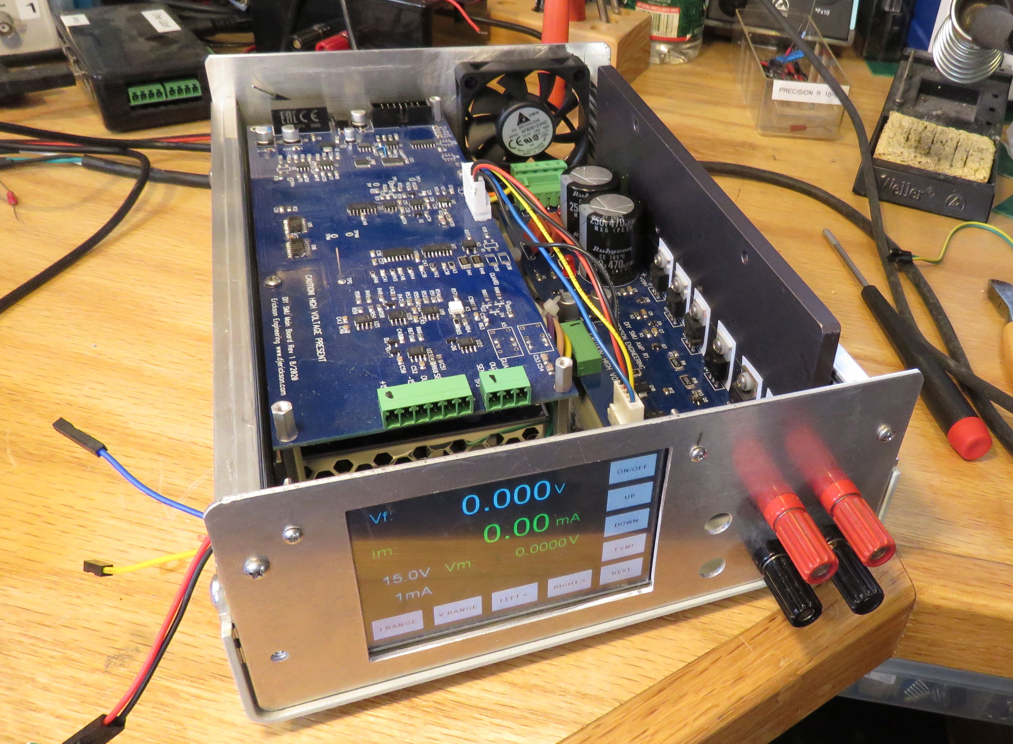
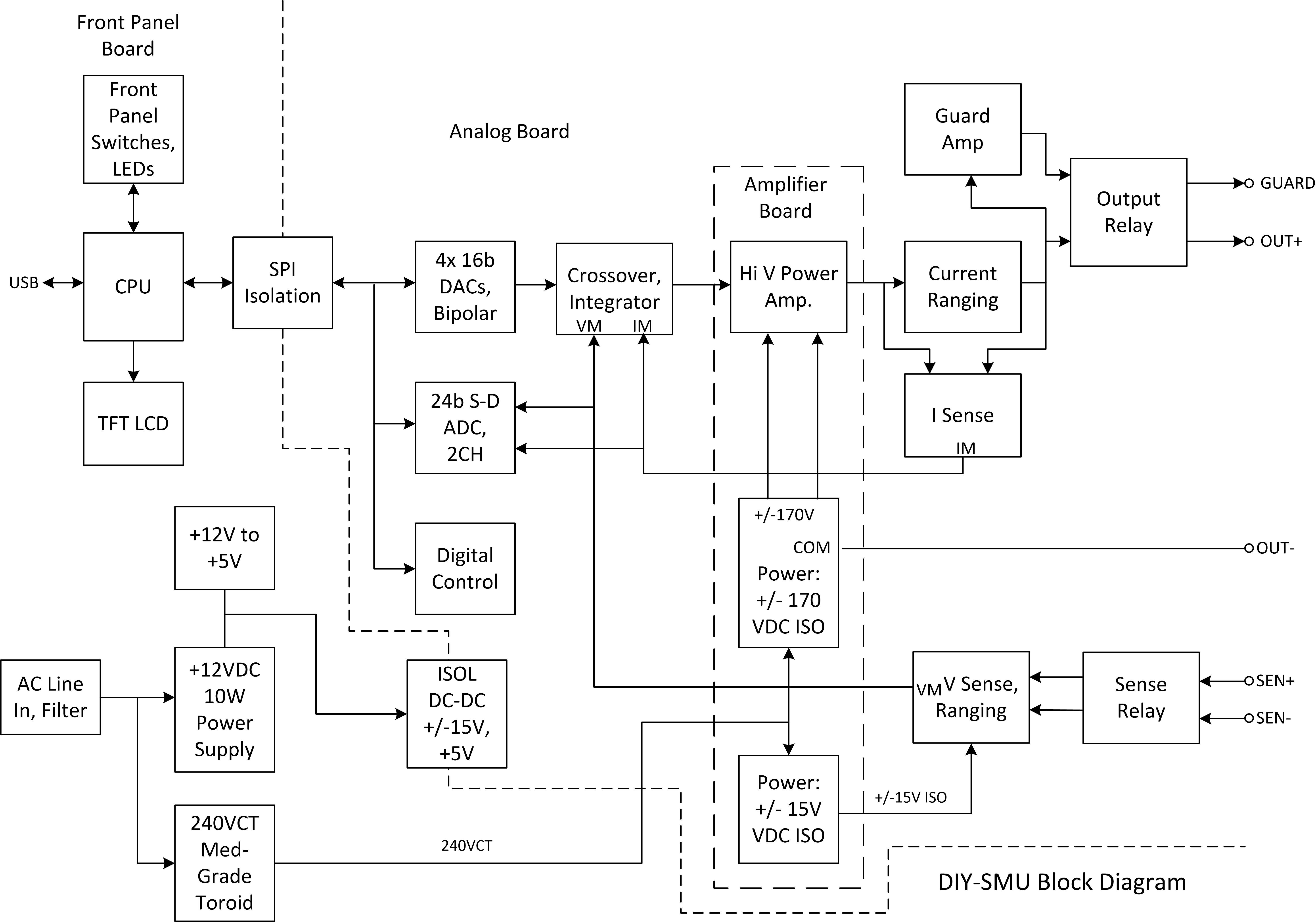
Block Diagram
Here is the overall block diagram.
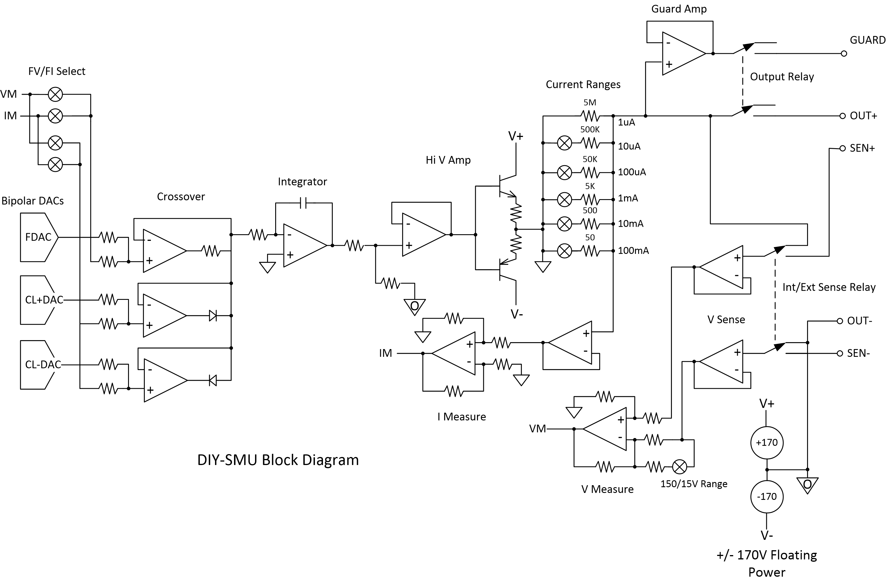
Here is the block diagram for the analog and power amp boards.
The general architecture is similar to the 236. The entire
instrument is floating with a guard to minimize leakage currents
and interference from external sources. Major systems are:
3 16b bipolar DACs for Force, High clamp
and Low clamp
Analog switches to configure either FVMI or
FIMV
Crossover to switch between force and clamp
control
Error Integrator
High voltage amplifier with floating +/-
170V power supplies
Current ranging from 1uA to 100mA full
scale
Current sense
Voltage sense with remote sense option
Simulation
I built up a simple simulation of the SMU in
LT-Spice. I already had a 3-op-amp crossover design left over from
the PS-Load project. The clamp circuit, power amplifier and
floating +/- 170V power supplies worked
well and with good transient
response. I simulated a bunch of
low current modes successfully. Time to build some hardware.
PCB Design
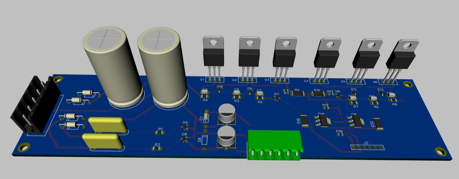
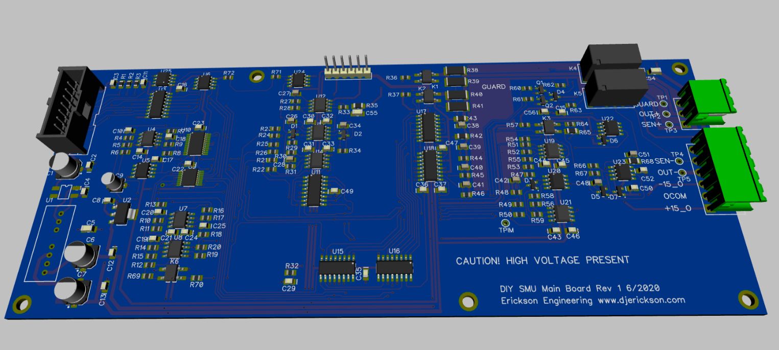
I designed the Amplifier and the Analog boards in
my favorite CAD tool: DipTrace. Here is the early version power
amplifier board 3D model.
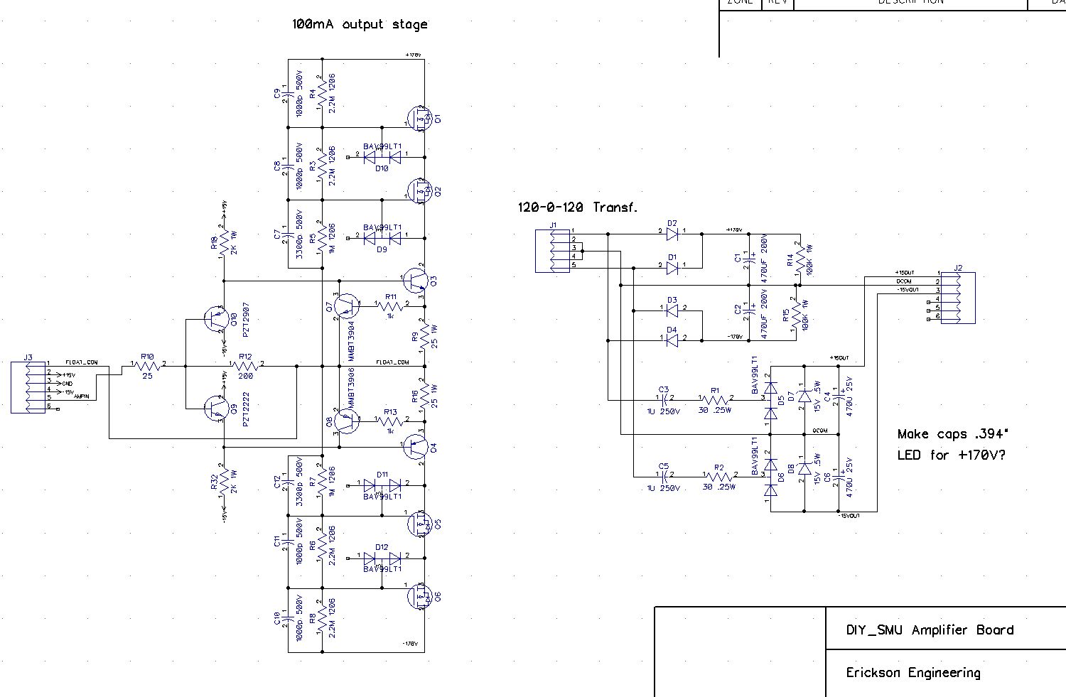
On the left side of the schematic is an early version of the
amplifier. The power NPN/PNP Q3 and Q4 control the currents in the
FETs. The R/C voltage dividers on the FET gates control the FET
voltage drops.
On the right is the floating +/- 170V power supply with the +/-
15V supply for the Voltage Sense amplifier. It is powered from a
30Watt 120/120VAC (240VCT) medical grade isolation transformer
with an electrostatic shield. It uses film capacitors to drop the
120VAC voltage to +/- 15V efficiently.
Here is the main Analog board. On the left is the SPI digital
interface, +/- 15V DC-DC, and isolation. Next to the right is the
References, ADC and DACs. Then the crossover, then the current
ranging, then the current sense, voltage sense, and guard
circuits. Top right is the output and sense relays, output and
sense connectors on the far right. Click for full res schematic in
.PDF
Crossover / Clamps
Clamping is required when the current or voltage
limits are exceeded. One good example is when sourcing current. A
theoretical current source without a clamp can go to infinite
voltage into an open circuit. A real-world current source will
eventually clip at some voltage, but that voltage may cause damage
or a latch-up condition. Setting clamp voltages to safe values
ensures that the voltage will be within safe limits.
FVMI means Force Voltage, Measure Current. FIMV means Force
Current, Measure Voltage. With FVMI the clamp current
settings are current limits, similar to a power supply, and
preventing the voltage source from outputting dangerous currents.
An example would be where a DUT fault causes a short circuit to
ground. It is important to limit the DUT current in this
case.
The crossover's job is to cleanly switch from current to voltage
control when a clamp occurs. I have designed and used a few
crossover designs in the past. Keithley
Patent 5,039,934 is for the crossover used in the 236. It
addresses both polarities of both current and voltage. In the old
days, 16 bit DACs were very expensive, but nowadays, not so bad.
The 236 uses two 14b DACs for voltage and current, and has an
additional bit to provide polarity control. Using a single
DAC for both clamp polarities means that both the negative and
positive clamp values are always the same but with opposite
polarity. This may or may not be a problem.
Another downside to the 236 circuit is that when a force polarity
change is made, the output can have a large transient. I don't
know for sure but I assume that when a polarity change is made,
the output is turned off during the transition. This is an
inconvenience when ramping from one polarity to the other.
Another downside is that the crossover uses four constant-current
diodes for the force crossover amplifiers. These parts are
expensive and hard to get. My design uses one resistor instead.
Another downside is the number of switches required to change from
FI to FV, and the need for a precision polarity control. Another
is the complexity of the compliance circuit . It uses four more
CMOS switches plus a dual comparator. Another is that the 236
requires zero setting correction hardware using the polarity
signals plus resistor-diode circuits for each crossover. If a
small 0 setting correction is needed on the DIY-SMU design, it can
be applied in software.
I think the 3 DAC, 3 opamp crossover is a bit simpler and more
powerful. I used it on the PS-Load project successfully. A single
bipolar DAC is used to set the force value, independent of FI or
FV. This has the advantage that if higher precision is needed
(better INL or more bits) then only one precision DAC is needed.
The clamp DACs accuracy are generally less important than the
Force DAC. The crossover input needs a 2:1 mux to select
whether the force error amp receives Measure Current or Measure
Voltage. The opposite is true of the clamp error amps. When
changing force modes, the two clamp DACs change values. The
compliance detect is simple: 2 comparators to ground on the clamp
op-amps. If either clamp error amplifier crosses 0, a clamp
(compliance) event is occurring. This signal is passed via a
separate isolator to the CPU.
With the 3 opamp design, one risk is that the + Clamp must always
be set to a higher value than the - Clamp. Otherwise the two clamp
op-amps will fight, and the output will swing wildly to the rails.
Don't cross the streams!
Current Ranges
DIY-SMU will have 6 decade current ranges from
1uA to 100mA full scale. Future versions may have a 1A current
range at lower voltage, like the 2400. The 236 applies +/-10V drop
across the current resistors. The 2400 uses +/-2.0V. DIY-SMU uses
+/-5.0V to limit resistor power and to still achieve high
accuracy. Precision resistors with 5xx and 4.99 values are readily
available.
The lowest current range, 1uA uses a 5 Meg ohm shunt resistor. The
highest 100mA current range uses 50 ohms. CMOS switches select the
resistors on all but the highest range. On that range a 1 ohm
photomos relay provides the switch. Sense for the resistors are
switched as well. All of the highest value resistors have a common
sense line since the switch resistance is negligible compared to
the shunt resistance. The higher current shunts have individual
sense lines selected by switches along with the range switch.
To achieve 1 part in 1000 resolution or better / accuracy on the
1uA range, the leakage current of the output stage must be less than 1nA. Since
there are many passive and active components and CMOS switches
connected to this node, the leakage of individual switches and
semiconductors current needs to be about 0.1nA. Leakage current
also increases with temperature, so keeping the temperature down
is good practice. I use low-leakage VIshay DG441 CMOS switches.
If it is necessary to have even lower than 1nA performance or <
1uA ranges, then relays or J-FETs will be needed. But with
reed-relays, it is important to watch the relay activation times.
CMOS switches change state in ~100 nanoseconds and so switch
control is simpler.
High Voltage Power Amp and Buffer
The high voltage amplifier is similar to the
236 design. It uses bipolar emitter-follower power transistors
whose outputs drive GND via emitter resistors. The collectors of
these transistors are (indirectly) tied to the +/- 170V power
supply. In reality, the +/- 170V power supply common terminal is
the output. It's a bit of a mind-twist to think about this. 15:1
voltage feedback is provided back the input of the buffer to set
this amplifier gain at -15. +/- 10V on the amplifier input
(integrator output) causes the output to swing +/- 150V. The
gain resistors stabilize the circuit with all types of loads
from 0 to infinity ohms.
To achieve an amplifier with +/- 150V of
output swing (300V p-p), 400V or higher transistors wold be
needed. The maximum power in these transistors is about 2 x 170V
x 100mA or 34W. This is do-able in single devices, but
unnecessarily challenging. Instead, the transistor voltages and
thus power dissipations are distributed in three devices, wired
in "cascode": one bipolar transistor plus two Power FETs in
series. A resistor divider string drives the FET gates and so
controls the voltage sharing between the three devices. Lower
voltage devices can be used in this manner.
Then the whole three-transistor plus resistor
string is mirrored with complementary devices on the - side, for
a total of 6 power transistors. Local current limiting is
provided in case of output short circuits or faults that are too
fast for the control loop to respond.
Heat sinking and forced-air cooling are
required for these devices. To use a single grounded (and safe)
heat sink, high voltage isolation of about 400V is needed on
each transistor. Unfortunately high voltage insulators also have
relatively high thermal resistance of about 1°C/W. So the 34W maximum
is divided by three devices, so each device temperature rise is
reasonable.
The power amp needs a high input resistance
and to drive the output transistors with about 5mA to output
100mA (beta 20 min.). I use a basic op-amp plus complementary
follower driver transistors.The drivers Vbe compensate for the
output transistor Vbe drops and so reduce crossover
distortion. The 236 and 2400 use a high-current buffer
amplifier and diode bias tricks instead.
Voltage Sense and Ranging
The requirements of the voltage sense circuit
are: stable performance from mV to +/- 150V, and pA bias current.
This low bias current is needed because of the low current ranges.
In order for the 1uA range to have >1000:1 dynamic range, the
leakage currents must be <1uA / 1000 or <1nA. The
SENSE+ amp sees only the +/- 5V across the shunt resistors plus a
few volts for the sense lead drop, so can be a 'normal' +/- 15V
op-amp. The SENSE- amp needs to buffer the output - voltage which
can be +/- 150V. Fortunately the +/- 150V floating power supply
can be tapped to obtain -VOUT +/- 15V to power this buffer. This
amplifier's low impedance output then drives a high resistance
30:1 divider, to reduce the measure voltage from +/- 150V to +/-
5V.
Needless to say these delicate FET pA op-amps need protection from
Bad Things like high voltage transients. Series resistors and
low-leakage BAV199 diodes, plus their on-chip ESD diodes should
protect them.
These two unity-gain buffer op-amps feed a differential amplifier,
similar to a normal 3-amplifier Instrumentation Amplifier.
To change the voltage range to +/-15V or lower, this divider ratio
is changed to 3:1. A Photomos switch can handle the 150V
need for this.
The 1.5V range uses the same 3:1 divider as +/- 15V, but reduces
the Force DAC voltage range from +/- 5.0V to +/- 0.5V.
ADC
Keithley, HP/Agilent and others generally use
custom designed, multi-ramp, integrating ADCs for their DMMs and
other precision DC products. I will use a modern delta-sigma ADC
instead. These can achieve 20 or more bits of resolution and
stability and can trade off resolution and noise level vs. speed.
The requirements are:
20-22 noise-free bits at 100Hz sample rate
Up to 1-4K sample rate at reduced
resolution
Pseudo-differential or full differential
External conversion from Bipolar +/- 5V to
Unipolar 0 to 5V
0 to 5V input range
2 to 4 input channels
The AD7190 meets these needs nicely. Like most
modern ADCs, the input voltage range is limited to 0 to Vdd. They
perform bipolar conversions by wiring the - input pin to a mid
voltage. such as the +2.5V reference voltage. Then low voltage
op-amps are used to convert bipolar voltages to the 0 to Vdd
range. By using precision rail-to-rail output op-amps, the input
range of the ADC can be safely met.
Calibration
With all precision instruments, some type of
calibration is required. In the old days trim-pots provided
calibration. Since the '80s however most DMMs use closed-box (no
trim-pots) calibration. Calibration correction factors are stored
in non-volatile memory. I intend to use EEPROM to store offset and
gain calibrations for each input and output range.
A standard issue with DIY equipment is that professional cal labs
may not be able to calibrate it, and even if they do, DIY's will
probably want to, well, DIY. My goal is to allow this unit to be
calibrated in a reasonable time with a 6.5 digit or better DMM
such as a 34401A. Maybe with some low-cost additional HW such as
precision resistors for the low-current ranges.
Power supplies
Several floating (isolated) power supplies are
required. On the 236, a custom AC transformer with 5 isolated
output windings, and multiple shields provides all of the required
voltages. On the 2400, a high-frequency transformer provides
similar functionality.
+12V grounded at
about 10W for the CPU, Front panel, Fan, and to power the
Analog Board
+5V Grounded linear
for the CPU and front panel
+/- 15V DC-DC, 3W
for the analog board
+5V for the Digital
logic, relays, ADC and DAC
+/- 170V Floating:
Main power output. Common is -OUT
+/- 15V Floating for
the -Sense Amplifier
One goal of this project is to avoid an
expensive, custom transformer. The grounded circuitry is
powered by a small, low power (10W)
+12V switching power supply. This
supply powers the front panel and CPU as well. The analog control circuitry uses isolated +/- 15V
and +5V. These are provided by a small 3 Watt DC-DC converter on
the analog board, powered by the +12V grounded supply. This DC-DC uses additional filtering and a common-mode
choke to minimize the common-mode output noise on the analog
ground.
The main output power source is from a floating +/- 170V supply
which powers the SMU output +/- 150V. A small 30-50W,
troroidal medical-grade isolation transformer is used.
Medical-grade transformers have an electrostatic shield between
the primary and the secondary. The shield helps to minimize both
leakage current on the secondary as well as power line common-mode
noise induced to the secondary. Ideally there would be two
or more electrostatic shields, one connected to the chassis ground
and one connected to the output common. I know of no off-the-shelf
transformers that have this. We will see if using a single shield
is adequate. Isolation transformers typically provide 120/240V to
120/240V. By rectifying a 2x120VAC (240VCT) secondary, +/- 170V
DC, unregulated is provided at up to 100mA.
This power supply common is the -OUT of the instrument. The high
voltage amplifier moves the ground around to vary the output
voltage and current.
The -SENSE voltage amplifier needs to measure the +/- 150V
output voltage with very low (pA) current. One way to do this is
to power a low-bias opamp from +/- 15V power with respect to the
-OUT terminal. To generate the +/- 15V for this amplifier, I use
film capacitors and Zener Diodes to drop the 120VAC to +/- 15VDC.
Capacitors are more efficient than resistors for dropping large
voltages at low current.
I recently learned that the original 236 circuit for +/-15V
causes a reliability problem seen on several old units. These
units use 15K ohm power resistors to drop the +/-150V to +/-15V.
These burn 1.5 watts and get quite hot, so require forced-air
cooling from the fan. But if the fan fails, the resistors can
overheat and fail, often shorted. Next to fail is the zener
diodes which fortunately fail shorted, saving the expensive
downstream precision circuitry. My capacitor dropper burns very
little power.
An advantage of the '236 design is that the 15K resistors are a
constant load on the +/- 150V supplies. So when the AC power is
removed, the high voltage capacitors discharge to 37% with a 7
sec. time constant (470uF * 15K). So the voltages are human-safe
within about 15 seconds. The capacitor dropper doesn't provide any
DC load, and the amplifier only provides only a 5Meg load, so the
high voltage can stay up for many minutes, creating a shock
hazard. To address this, I use a 100K "bleeder" resistor on each
+/- 170V supply to draw 1.7mA and consume 0.3W. This is still a
long time constant but much shorter than without the
bleeder. These resistors feed two red LEDs that light when
the power supply is dangerous. I may add lower value resistors to
burn a bit more current and make the LEDs brighter.
Update 3/28/21: Detailed Explanation of the
DIY-SMU and 236 Amplifiers
Here is a simplified block
diagram showing the overall DIY-SMU amplifier design. The BUF
stage is PNP/NPN transistors. See the schematics above for
details.
There is a lot of subtlety in the Keithley 236 / DIY-SMU
amplifier. The design uses a bipolar transistor and FET stack to
convert a low voltage input to a high voltage output. It does this
in a clever and non-intuitive method: Instead of the amplifier
driving the +Output directly, the +/- 170V floating power supplies
of the amplifier are driven indirectly by the current outputs of
the +170V and -170V amplifiers. This has the effect of causing the
+/- 170V common terminal to change. This terminal is the -Output
of the instrument.
There are other circuits required to make this work:
1) The amplifier has a current output (high impedance) as opposed
to most amplifiers which are voltage output, low impedance. The
gain and frequency response of a current output amplifier is
highly load dependent. To drive and stabilize it, there is local
feedback for a voltage gain of x-20. This is provided by resistors
R35 (200K) and R33 (10K) via buffer opamp U12.3. The buffer
and the gain setting resistors for the amplifier are on the Main
board on both the 236 and the DIY-SMU. The overall amplifier
circuit is basically a big opamp, wired for an inverting gain of
x-20. But, unlike most opamps, the loop gain is high only for high
impedance loads. The current output nature of the amplifier causes
a fall-off of the closed-loop gain with lower impedance loads.
2) To get a low bias current -Sense input for the -Output, the
-Sense op-amp is powered from +/-15VOut supplies, referenced to
the -Output. This allows it to buffer the -Sense input over a
range of +/- 150V safely and still maintain pA input (bias)
current. Because of the potential high voltage input range, diode
input protection and output current limit are required for this
amplifier.
3) Local, fast, output current limit is required. This consists of
transistors that measure and limit the current in the main NPN and
PNP transistors in the case of excess current. To protect other
circuitry such as the current ranging, 2 limit settings are
required: ~ 130mA for the 100mA range, and ~15mA for all the other
ranges. MOSFETs are used to switch this current limit as a
function of the current range setting.
4) Bias and buffering. The 236 amplifier uses an old LH4001 Hybrid
buffer IC to drive the output transistors. It uses bias diodes and
resistors to minimize crossover distortion. The 2400 uses a AD847
fast opamp in the place of the LH4001. It is the only DIP IC on
the board. I believe they used a DIP to increase the power
dissipation.
DIY-SMU uses complementary transistors driven by an op-amp to
drive the amplifier, minimize crossover distortion, and to replace
the expensive buffer IC.
To really understand the amplifier, study the 236 service manual
in detail, and build a Spice model for the amplifier. Spice will
easily simulate the floating +/- 170V and +/- 15V power supplies,
but I haven't figured out how to model the -Sense buffer's
floating power supplies with an op-amp. I use a behavioral model
instead, an ideal voltage-to-voltage source. My LTSpice model is
the .ASC file is in the .ZIP file above.
BTW the 236 has a closed-loop gain of x-11.0 on the 110V and lower
ranges, and x-110.0 on the 237 1100V range. These assume +/- 10V
input from the integrator. DIY-SMU's x-20 gain may be higher than
needed for its +/- 150V output.