![]()
![]()
![]()
![]()
![]()
![]()

|
|
MicroBus: an I/O bus for embedded systems.MicroBus is a new, modular, open interconnect standard for embedded microprocessor systems. It allows standard or custom peripherals to be added to a system quickly and easily. MicroBus allows either standard flat cable or a hard mini-backplane for interconnection. It's flexible packaging allows boards to be stacked vertically or mounted in a horizontal plane. MicroBus small board size and easy interfacing help keep system costs down and make it the lowest cost expandable bus standard available. MicroBus is simple to design to and allows peripherals to use either byte-wide, clocked serial or I2C devices. A typical interface can be implemented with a few simple logic devices or a single low cost PAL device. Advantages of MicroBus
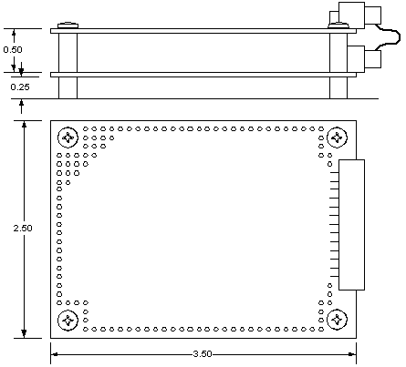
Why MicroBus?Certainly there are other computer busses available. VME, PC104, CPCI, STD and other standards are widely available. These busses are designed for high end systems and their size and complexity reflects this goal. It is difficult to configure a VME or CPCI system consisting of three boards for less than about $5000. In PC104 a typical minimum system is about $300. In addition these systems generally require a complex operating system that drives up Flash and RAM memory cost. System Cost One important consideration for any system is the minimum incremental cost to add a single, simple function. I call this the "Blinking LED" problem, or "How much does it cost to implement an additional function with a single blinking LED?". This question effectively asks "What is the bus overhead cost?" The answer in the case of CPCI or VME is a full or half size 4 layer board, the card cage board slot to accommodate this board, the front panel ejector hardware, a complex bus interface with its development cost, unit cost and markups. Our estimate is that a 6U VME blinking LED board and its chassis slot would cost about generally in the range of $700 and a half size 3U CPCI board about $400. Ouch!. Clearly such a board is not practical and the tendency would be to add other functions to the board. This drives the cost per function down, but the board cost up. In a stacked PC104 system the "Blinking LED" board would not incur a backplane slot and the relative simplicity of an ISA bus interface could be implemented on a 16 square inch 2 layer board. But board size and bus complexity would still cause a board to cost about $100 including markup and defraying the development costs. Obviously a blinking LED could be implemented in other ways, but the costs for other simple functions such as a handful of parallel I/O bits, one more UART, or an alphanumeric LCD and keypad interface would be comparable. So the result is that low end systems are generally full custom systems that incur hardware development costs. This is fine one has the time, budget, and talent for hardware design, component selection, board layout, debug, driver development, manufacturing, production test development, etc...The non-recurring costs must be spread out over a large number of units. Not a good business model when volumes are low and time to market is short. It is our opinion that a range of applications could use the advantages of modular plug-in boards for rapid development if the unit costs were not prohibitive. That the cost to develop and build a single simple function (Blinking LED) should not be prohibitive. And that the mechanics of a system should be flexible to allow the electronics to fit the system. Thus MicroBus. Board cost By keeping the bare board cost, bus electronic and mechanical costs low, the "Blinking LED" problem can be solved. Meanwhile the current state-of-the-art allows complete microcomputers with digital I/O, analog I/O, communication and timers all on a thumbnail sized device. So small board size is a strong advantage here as well. State of the art assembly using tiny device packaging, multi-layer boards and double sided SMT assembly can allow small boards to pack lots of functionality. Each of these technologies costs, but when density is important, these techniques can be brought to bear. Mechanical Considerations The board size for MicroBus is a credit-card-sized 2.5" X 3.5". With boards this size, I/O connectors up to 50 pin 0.1" and 100+ pin high density connectors can be used on the two long edges of the boards. Mounting of each board is with four simple male-female threaded hex spacers. This allows boards to be stacked easily and assembled with simple hand tools. Mounting is rugged and simple. Board spacing is 0.50" to allow I/O connectors as high as 0.375" to fit on each board. For higher components or or boards with daughter boards, two slots or 1" spacing can be used. The interconnect is designed to use either 0.050 pitch flat cable and female headers or a hard backplane. MicroBus MechanicalMicrobus is designed to efficiently implement modern semiconductor technology. Board size is kept small to allow single chip or multi-chip functions to be implemented on a single board without wasting board real estate or driving costs up. The interconnect used is a simple 26 pin 0.1" connector. systems can easily be configured with a soft backplane (ribbon cable), a hard backplane (PC board and connectors) or no backplane, in the case of a single board system. Boards can be mounted either vertically stacked or in a horizontal plane. This drawing shows the MicroBus board outline and two boards stacked with flat cable interconnect for MicroBus. The partial hole pattern shown is representative of PROTO1.
MicroBus SignalsMicrobus uses a simple parallel 8 bit bus for data transfer. It incurs very low overhead on both processor modules and I/O modules. It provides a data transfer bus, device addressing, a few important control signals, and device power supply.
All signals can be either 5V or 3.3V switching. All receivers must be 5V tolerant.
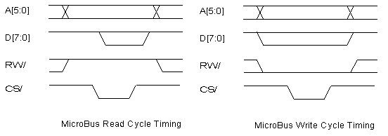
MicroBus TimingThe MicroBus uses very conservative timing to allow simple combinatorial logic to generate write and read strobes on each I/O card. The fundamental cycles are eight bit data read and write cycles to a single address. Serial cycles are comprised of multiple read or write cycles to a single address with only a single data bit valid.
To generate eight register read strobes, the only logic needed is a single 74HCT138 style decoder and a three bit equality comparator. The same is true to generate eight register write strobes. Read registers can be simple tri-state buffers. Write registers are simple D type registers. Many clocked serial devices require a data In and/or out line, a clock, and a chip select or enable, or load pulse. These signals can be easily derived from MicroBus control signals. Clock pulses and load pulses can simply be decoded write strobes. A serial data Input (to a device) can be one or more data bus D[ ] signals. For a serial data out, a single tri-state buffer can be used. A chip enable that must remain asserted for an entire serial sequence can be a single register bit. In this way, serial devices such as A/D and D/A converters, display devices, etc can be easily and efficiently interfaced to MicroBus. C language functions MicroBusR (char address) and microBusW (char address, char data) are used to initiate MicroBus cycles. Motorola Vs Intel Bus SignalsMotorola style interface chips use a R/W line to indicate whether a read or write cycle is happening. They use a single strobe signal to indicate the beginning and end of a cycle. In the old 6800 days this was derived from the bus clock signal called 'E'. This signal was gated with the appropriate address wires to enable each peripheral. Intel 8080/Z80 and PC ISA Bus type peripherals use two signals: IOR/ and IOW/ to indicate read and write cycles, respectively. The differences are simply conventions. Microbus uses the Motorola style interface because controlling bi-directional bus buffers is simpler. The control signals to control any Intel style peripherals can be generated from MicroBus signals by simple gating logic. MicroBus ElectricalMicrobus electrical loading rules are very straightforward. Each I/O board is allowed up to two CMOS loads on the bus lines. Beyond two loads it must use a buffer. Up to 12 boards can be used in a system. The maximum DC load on any board is 100uA, necessitating all CMOS for bus receivers. All receivers must detect logic high as 3.3V and 5V meaning that 5V receivers must be TTL compatible and all 3.3V receivers must be 5V tolerant. Use 74HCT instead of 74HC. All 5V and 3.3V programmable logic meets these constraints. All 5V and 3.3V pins must be bypassed to ground with 0.1uF bypass capacitors. this makes each power pin into an AC ground pin to help reduce ground bounce on the bus signals. Each data wire (D[7:0]) and the interrupt (INT/) has a single pull-up resistor on the master board to prevent floating CMOS levels. Plug and Play ???To design MicroBus as a Plug and Play bus was appealing. No jumpers or DIP switches to set wrong. However the overhead necessary to implement a plug-and-play structure is complex and therefore expensive. But Jumpers and DIP switches? That's so very 80's. What to do? What makes a bus Plug-and-Play is a mechanism to uniquely identify each board, it's manufacturer, type, base address(es) and it's system requirements. The plug-and-play concept was designed and made popular in the late 80's on the NuBus, which was adapted by apple for their high end Macintosh machines. PCI bus adapted Plug-and-Play. Around the same time the ISA Plug-and-Play consortium started up so newer ISA cards could eliminate jumpers. All of these protocols are fairly complex. Busses designed from the ground up use 'geographical addressing' using a unique per-slot, non-bussed signal on the backplane to identify each board by its slot location. This technique is used on NuBus PCI and VXI bus. To add Plug-and-Play to the existing ISA bus without any mechanism in place, it was necessary to do it within the constraint of the original bus. The clever folks on the ISA P&P crew found a sequence of bus operations 'not found in nature' that, when executed by a PC and followed by an address sequence, each P&P board would then identify itself and then cough up it's ID and system requirements. The OS would then allocate those resources to the device. In the case of ISA bus, this complexity adds thousands of gates of logic to the bus interface as well as significant driver software complexity. Most PCI bus interfaces use 5-10K gates also. To keep MicroBus simple, a way was needed to help eliminate address conflicts but that added virtually no cost. The baseline requirements are:
The configuration system is very simple. Each I/O board has a small DIP switch located in a consistent location on its board edge so that all DIP switches within a system can be quickly set and read. Conflicts can be easily seen by looking down a set of DIP switches for boards set to the same address. In addition each system has a simple label that identifies each board model number and address switches. Wouldn't PC life have been easier in the old days with such a system? Plug-and Play (affectionately known as Plug-and Pray) is a definite advantage to non-technical PC users to allow them to add and change hardware. MicroBus systems will typically be designed by engineers and configured by technicians who can read and understand DIP switches. So the answer to the Plug-and-Play question is that despite the benefits Plug and Play could provide, MicroBus will use a simple, intuitive and human-readable configuration process instead. MicroBus Power SupplyMicroBus systems are designed to require only a single +12V unregulated (or regulated) supply. Possible sources are unregulated wall-wart transformers, regulated +12V supplies, and 12V battery backed-up supplies. The voltage requirements are11-16V nominal. Possible sources are unregulated wall-wart transformers, regulated +12V supplies, and 12V battery backed-up supplies. The current requirements are dependent on the processor and I/O modules used but are typically well under 0.5A, For example, the RAB1 processor with Ethernet uses about 80mA of +12V. The processor board uses low cost switching and linear regulators to generate the other two bus voltages, +5V and +3.3V, to be used by the processor and I/O modules. See the Processor Board specifications for power use and power available to MicroBus. Typically a switcher will be used to generate the +5 and a small linear regulator will be used to drop +5V to +3.3V. Most I/O boards will operate directly from the bus supplies. Other supplies can be derived from the existing supplies. If an I/O board uses more than about 50mA of +5V or +3.3V, it should draw it's power from +12V and use a local DC-DC converter for its supplies. MicroBus Hardware Example: AVR MasterSingle-chip microprocessors may not have the data and address busses required for MicroBus. They usually do have the reset and general purpose interrupt inputs. MicroBus can use as little as one eight bit bi-directional data port and two additional output signal. The six bit address and R/W line are generated from the eight bit port by using one of the other two output bits as a strobe that latches the address and R/W line into an eight bit latch. The CS/ line is the other output bit. The schematic of a MicroBus Interface tied to an AVR micro is shown. Schematic Here The cost of the eight data bits on a processor with limited I/O may seem a high cost, but when you consider that: some systems already need an eight bit bus to communicate with a peripheral device (chip. LCD, etc) and those eight bits now can be expanded to up to 8 X 64 or 512 bits of I/O control, the cost is acceptable. MicroBus Hardware Example: Slave I/O PortA simple slave eight bit output port for MicroBus consists simply of a high address comparator, a low address decoder, and an eight bit D register. Output registers are strobed off Write bus cycles (R/W = 0). Eight bit read ports are simply tri-state buffers enabled by a decoded read strobe. Note that in the example, the single 74HC138 address decoder is used to decode four read strobes and four write strobes. Also that the write register is reset to 0 on power on reset by /RES. If this is not desired, then disable the reset pin on the register or use a register without reset facilities. It is generally desirable for an output port to power up in a known state though. Schematic Here The recommendation for MicroBus is to have only two CMOS loads on each data and address wire. In the case of the data bus, a bi-directional buffer may be desirable. If so its Enable/ should be tied to CS/ and it's direction should be tied to R/W.
|
|
Copyright © 2003 Micro Boards Inc.
|