Teardown
and Repair of a 850W Power Supply from the '80s
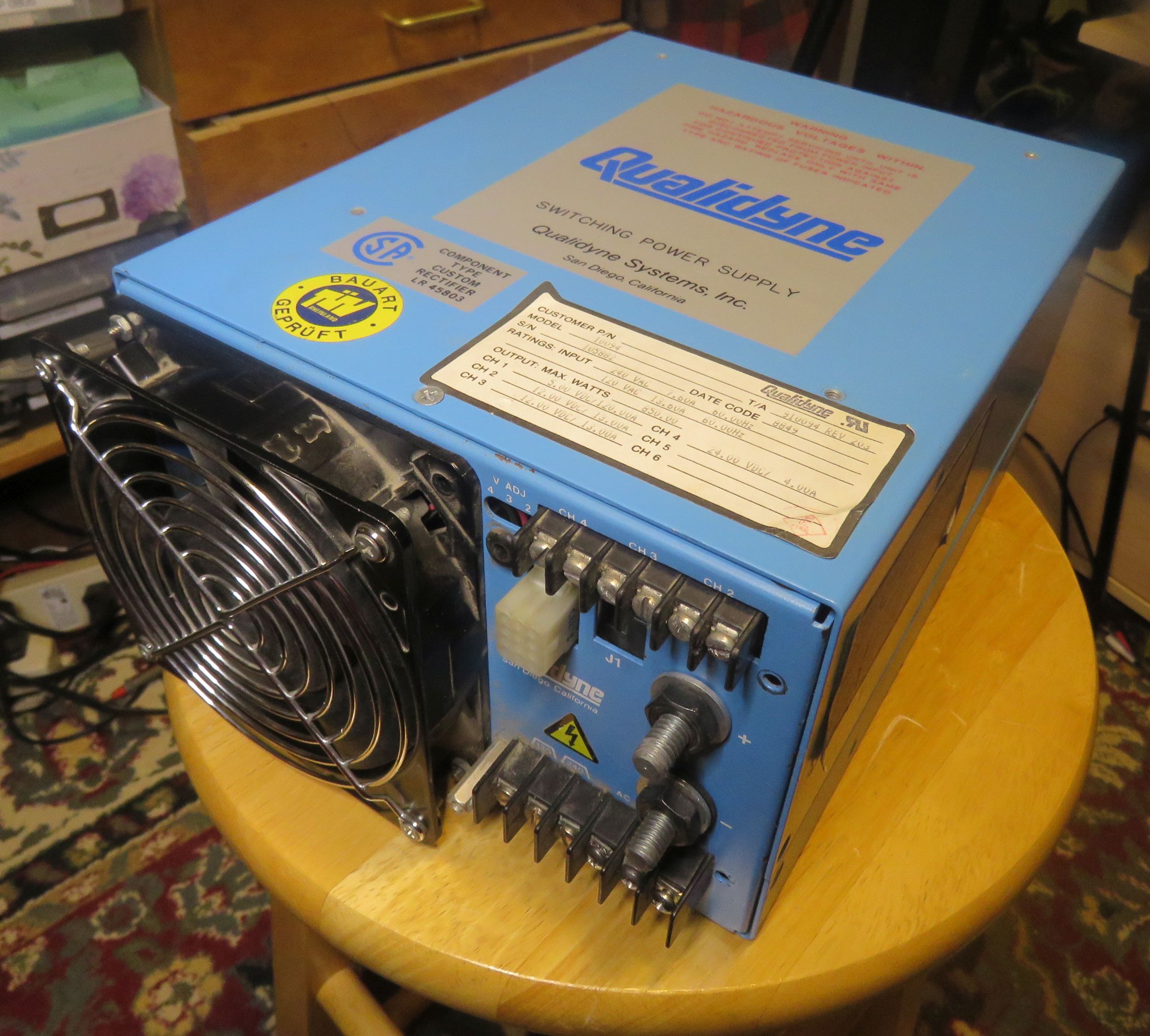
Qualidyne
10094, 5V, 120A + 3 Auxiliary Outputs
By
Dave Erickson
Intro
I was about to
toss this broken power supply into the E-waste bin. It was from a
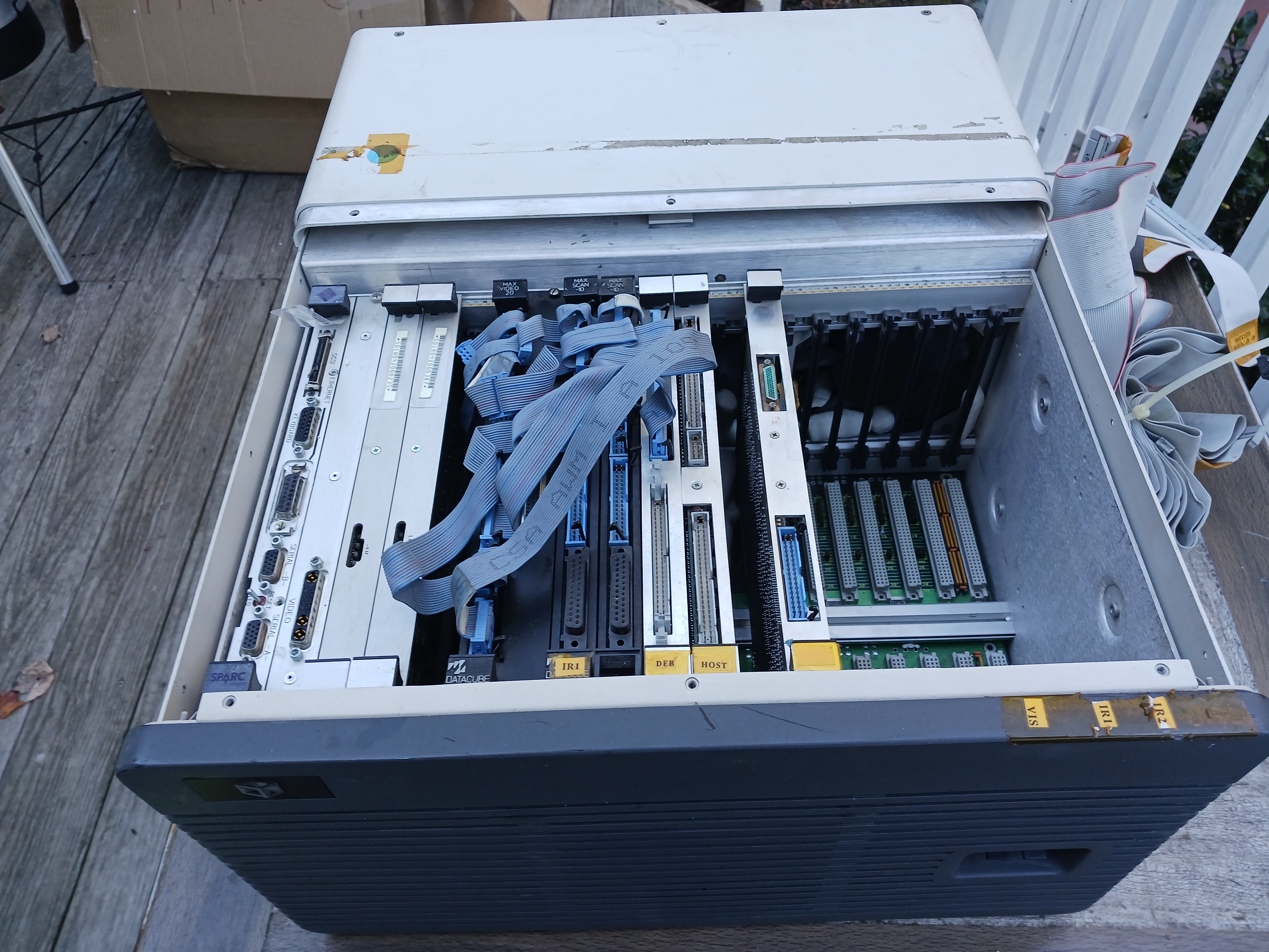
Datacube MaxBox 20 slot VME chassis. When I powered it up, the +5V
output voltage was +4.2V. I found a loose component inside it,
re-installed it, and messed around a bit, but the unit went from
almost working, to fully dead. I pulled this beast out and
replaced it with a spare PC power supply. I put the old power
supply aside, waiting for E-waste day.
But
I could not just toss it. I thought that some useful knowledge and
possibly some useful parts could result from a tear-down. After
removing the cover I saw that it was not easy to access the
components on the main board. The different assemblies inside were
all hard-wired together. A teardown would require significant
un-soldering of wires. As I have absolutely no use for a 1980's,
5V, 120A, 850W, four output power supply, I didn't feel bad about
scrapping it for science. Maybe someone will learn something.
The
supply was made by Qualidyne, its date code is "8849", so late
1988. One year younger than my daughter. I was the designer of the
MaxBox at Datacube, and specified
this power supply for the design about 1987. We built about 100
MaxBoxes. Later, Martin-Lockheed requested a militarized version
of MaxBox for their Lantirn IR
targeting system for the F15 and F16. They had designed about
8 MaxVideo-10 VME boards into the Lantirn test and calibration
system. These test systems were required in each air base that
deployed Lantirn. We designed a new ruggedized MaxBox chassis to
their specs and sold about another 100 systems to Martin. This
cash cow helped pay our 80+ employees salaries for several years
in the 90's. Each MaxBox and Martin system had one of these
Qualidyne Power supplies. It's an old friend.
The
power supply specs are:
- 5V at
120A
- +12V
at 13A
- +12V
at 13A
- +24V
at 4A
- 120/240VAC
- All
outputs are floating.
- Remote
sense on each supply
- 850W
- Various
status and controls
- Standard
5" x 8" x 10" enclosure
Unlike most
modern multiple output power supplies today, all 4 outputs fully
regulated and individually current limited. And all isolated from
each other. This is the classy and more expensive way to build a
power supply. I think we paid about $800 for these supplies, about
a buck-a-watt.
Here is a MaxBox 20 slot VME chassis. The power supply lived in
the back.
Repair?
I removed the
covers and soon discovered that the supply was quite difficult to
troubleshoot without a schematic and parts placement. With the
main +5V not working, the next thing to do on a typical power
supply is to check the main DC capacitors for +320VDC. That was
fine. That indicates that the AC fuse, input filter, rectifier and
main caps are all OK.
Next is to check the main controller. Typically one would check
that it is getting DC power and that its reference voltage and oscillator are working. Then
look at the DC inputs and the pulse outputs. That all assumes that
you know what IC it is and you have access to its pins.
Unfortunately I only had access to the bottom of the board. No
access at all to the component side: the giant output diode heat
sink and output caps completely covered it. Unfortunately
all this circuitry is buried directly under the main diode heat
sink, and is all screwed together. From the solder
side, I could see a single DIP IC, most likely the main
controller. I didn't know what IC it was, but an intelligent guess
would have been either a TL494 or a SG3525, popular1980's PWM
controllers. That would have gotten me very close. It's actually a
SG3527, a SG3525 with inverted outputs.
Here is the top level schematic I drew, once I got the diode heat
sink and main transformer off. Due to the 4 switching transistors
and the nearly 1KW output, I assumed a full H bridge. I was
confused by the base drive transformers. I could clearly see only
one high-current secondary (base drive) winding on each
transformer. How to control 4 transistors with only 2 base
drive windings? I later solved this mystery. It's a half bridge,
not a full bridge. The high side and the low side each consist of
two transistors connected in parallel. That also explains the
large film capacitor in parallel with a beefy 200 ohm resistor.
They connect the transformer primary and the heat sink to the
neutral / common of the power supply.
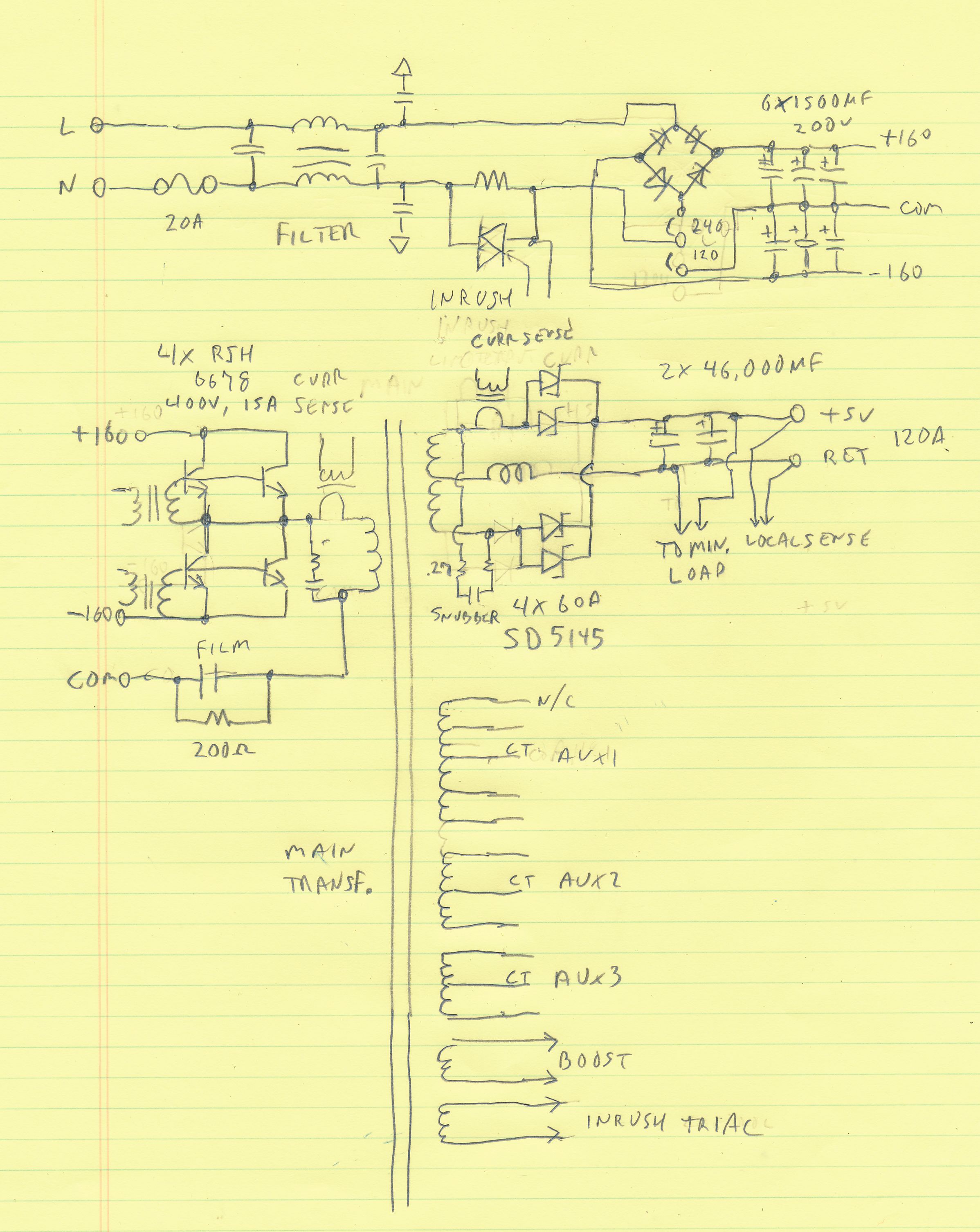
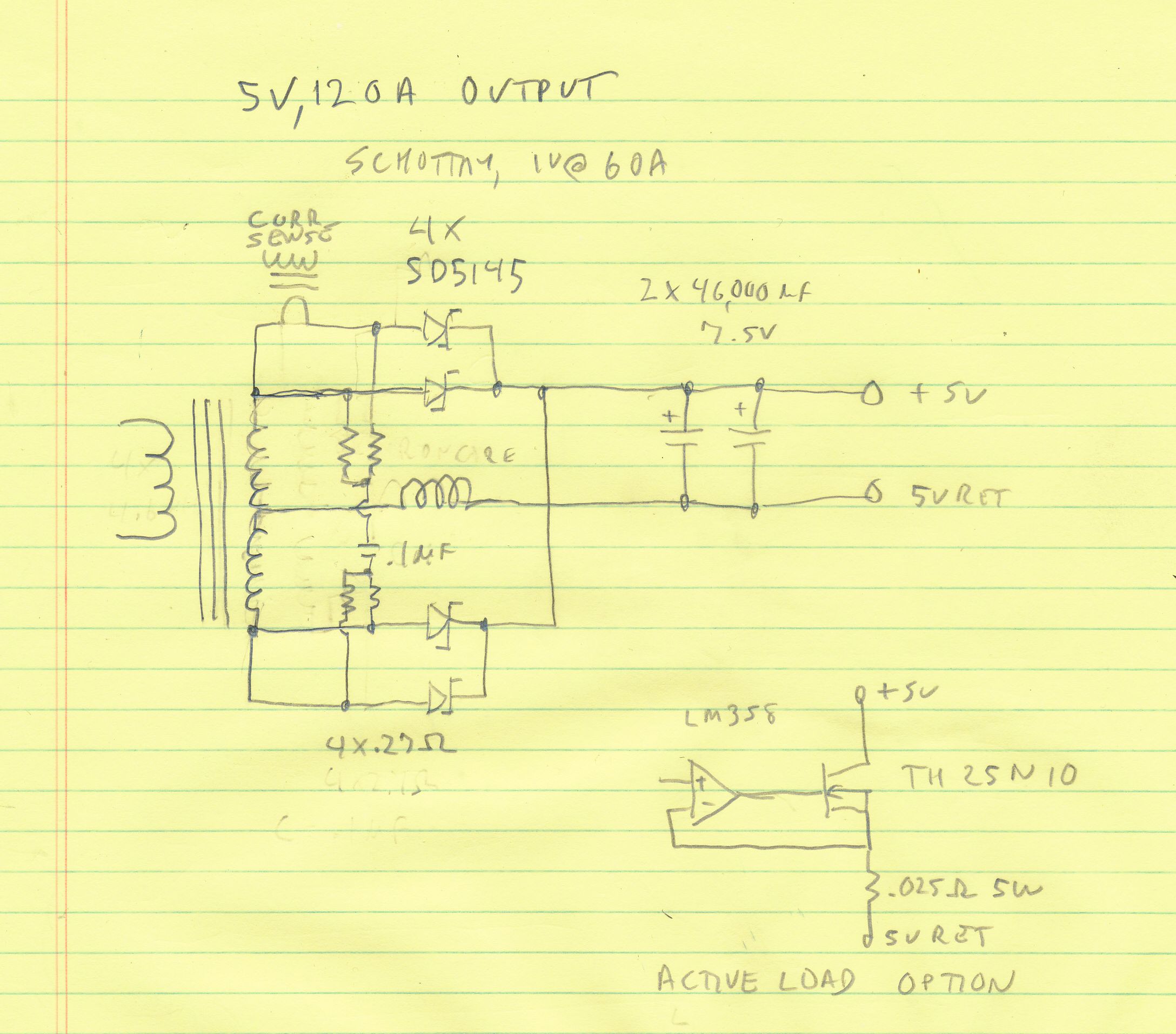
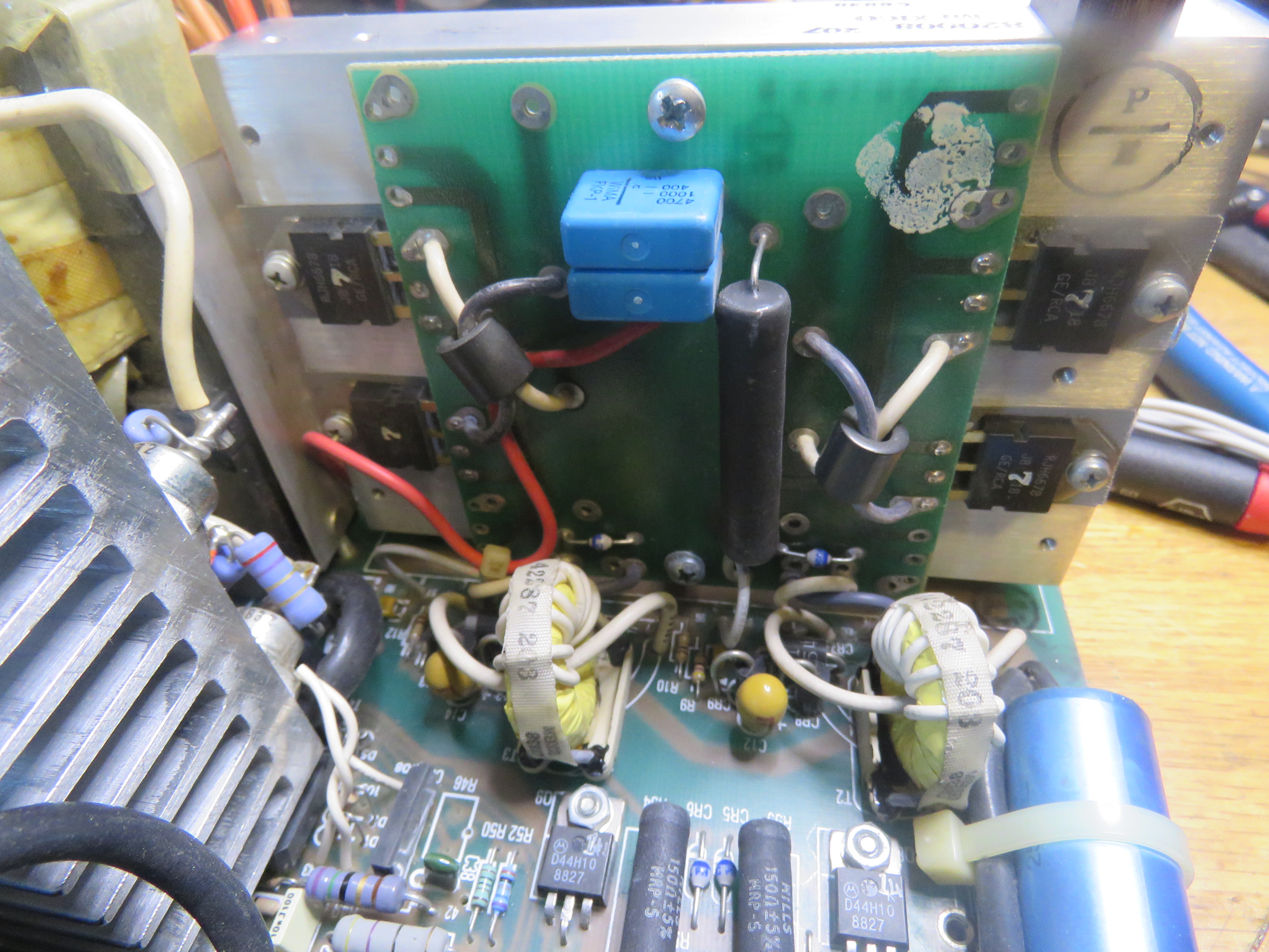
And
the main +5V 120A output stage. The current transformer actually
senses 2 parallel diode paths.
The
electronic load board provides the minimum load required by the 5V
supply.
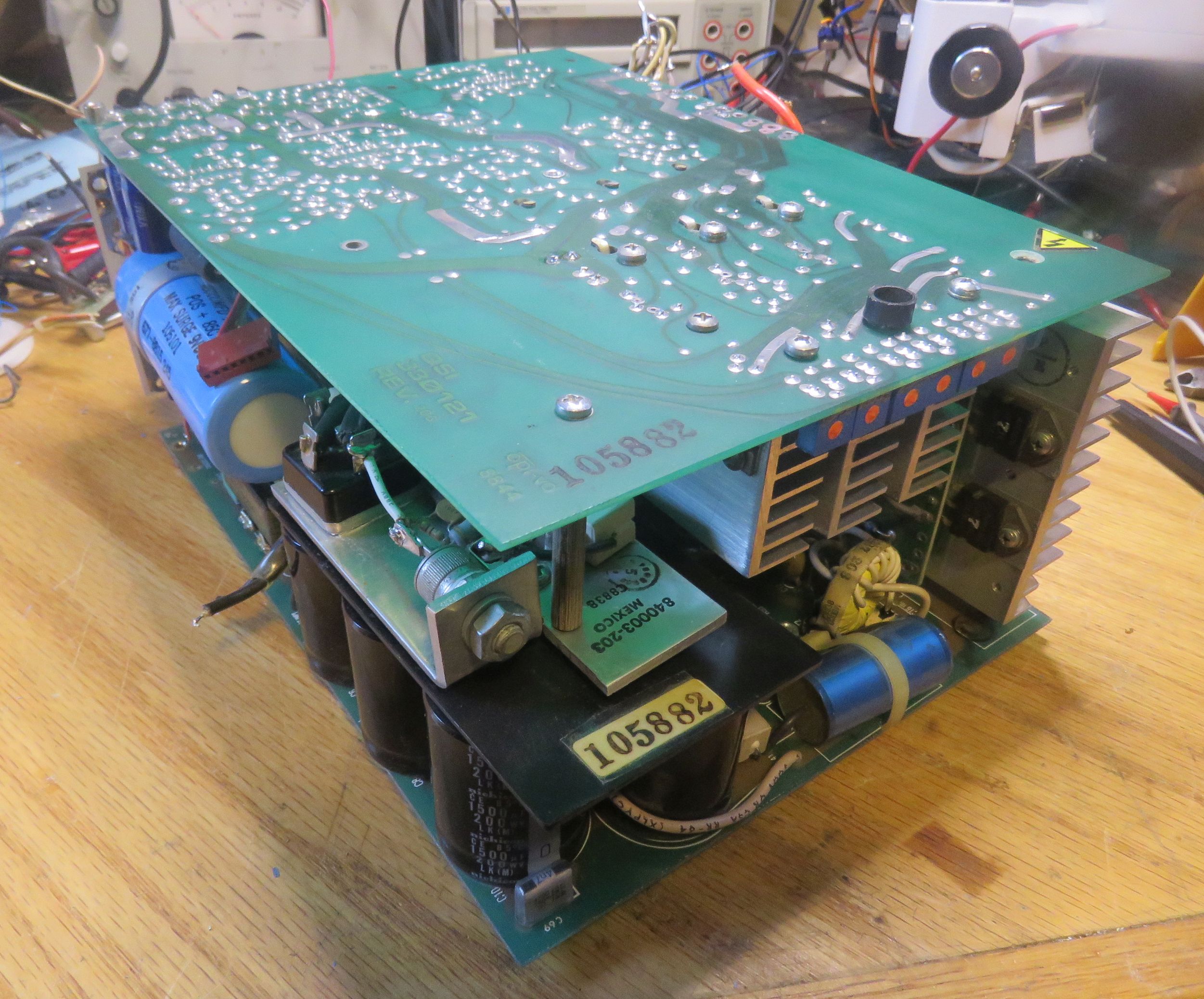
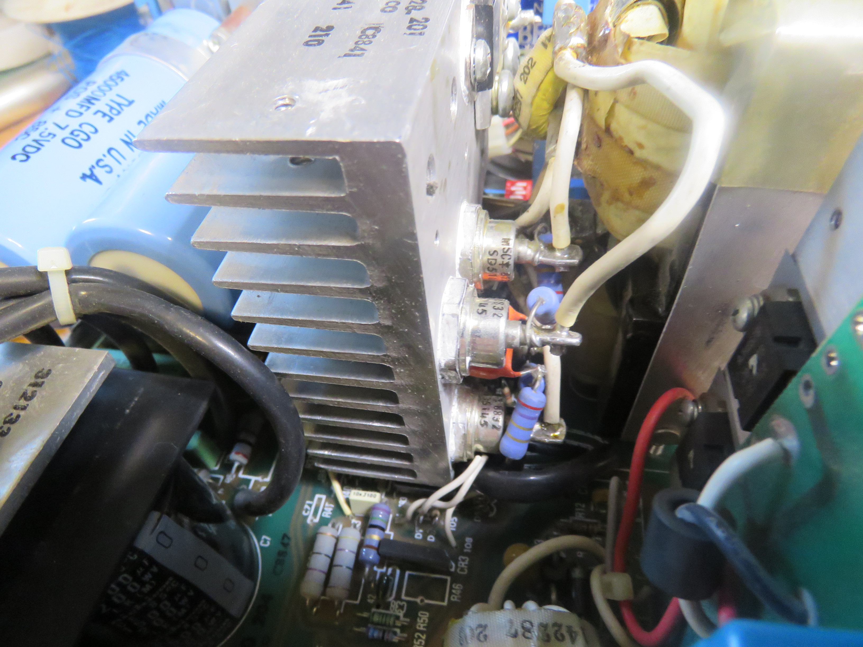
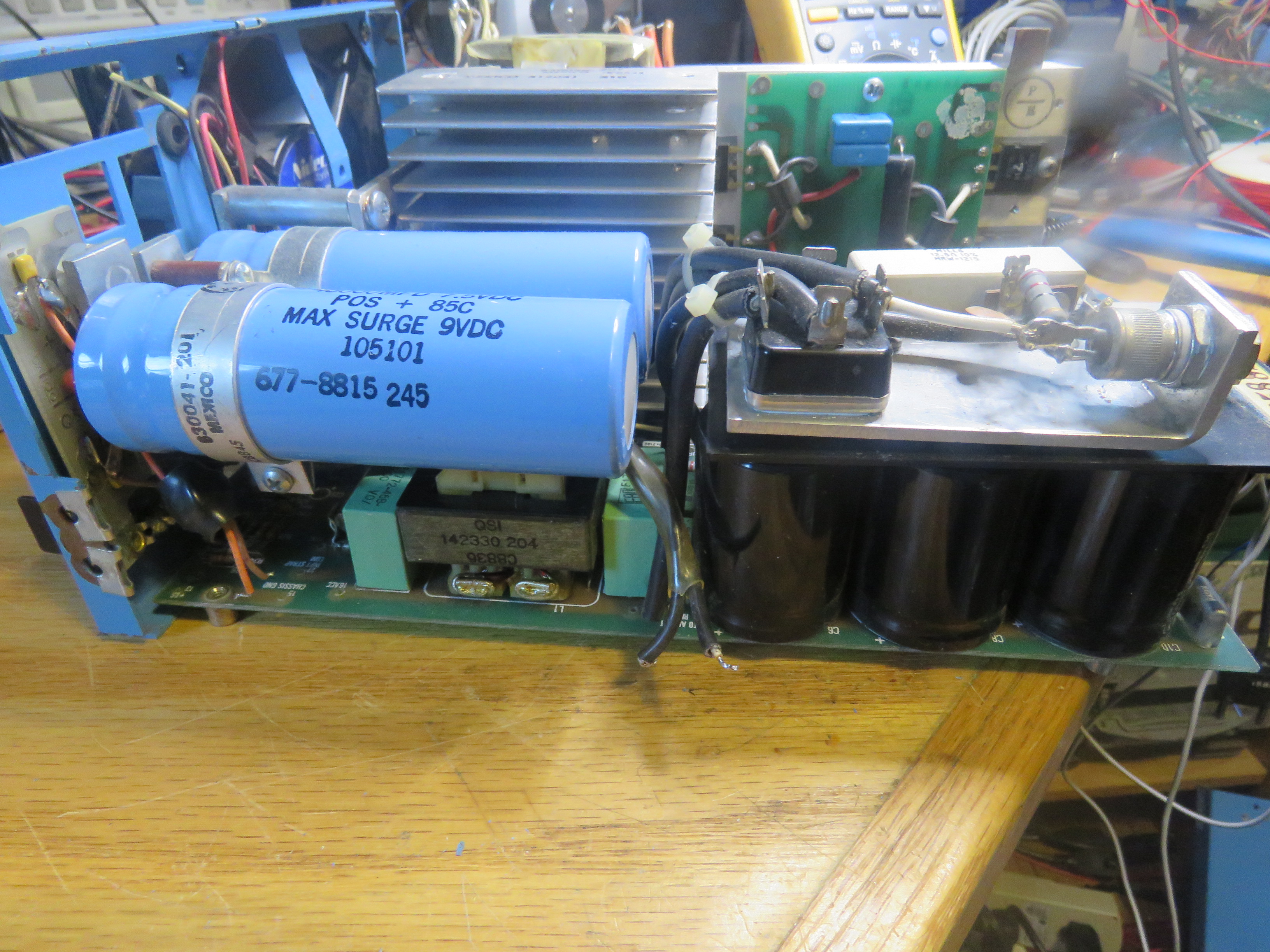
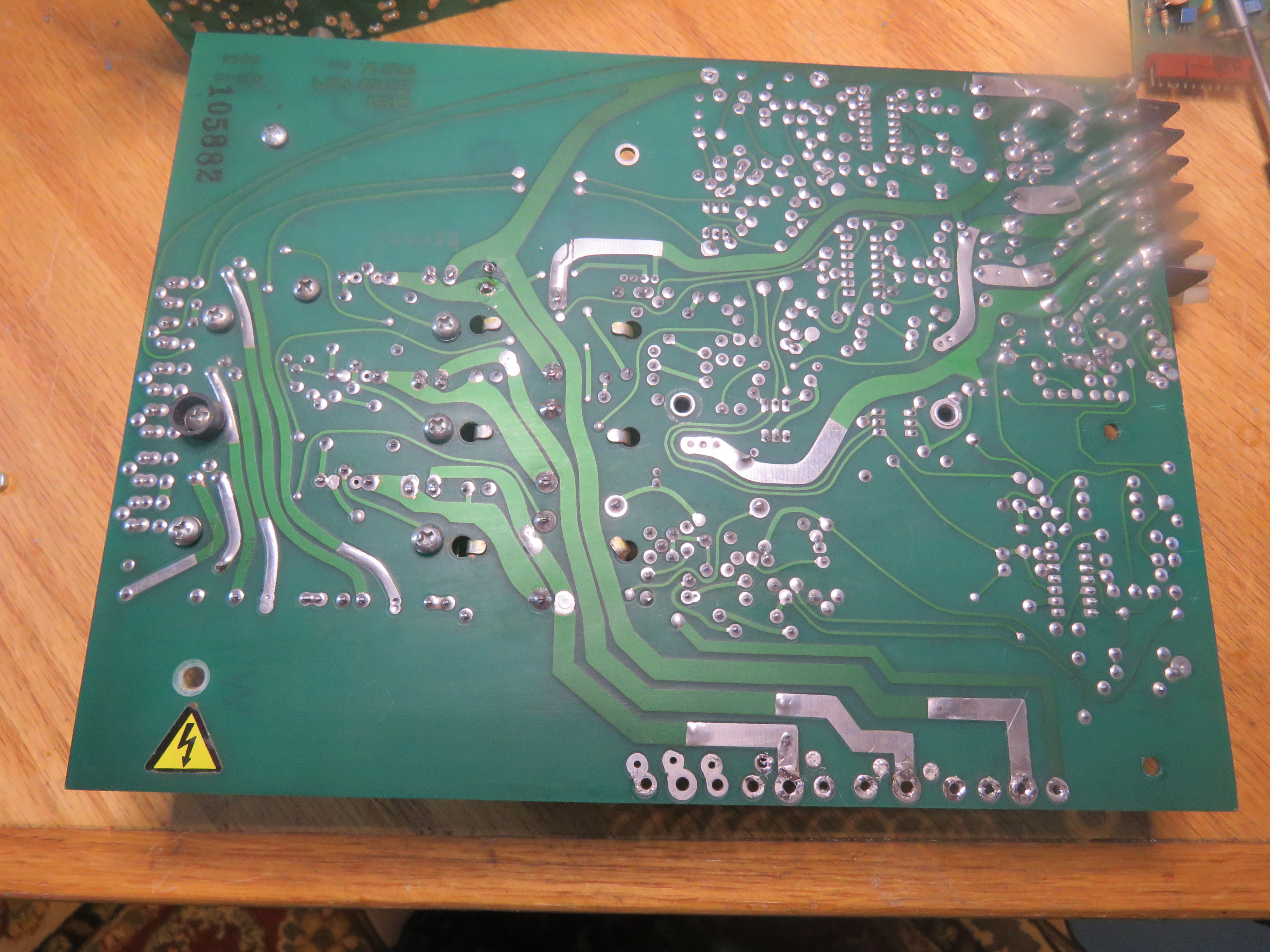
This is the original configuration, with covers removed. The
bottom board contains the AC in, Filter, main caps (black),
H-Bridge (right) and all the main controls. The top board is the
three Aux supplies.
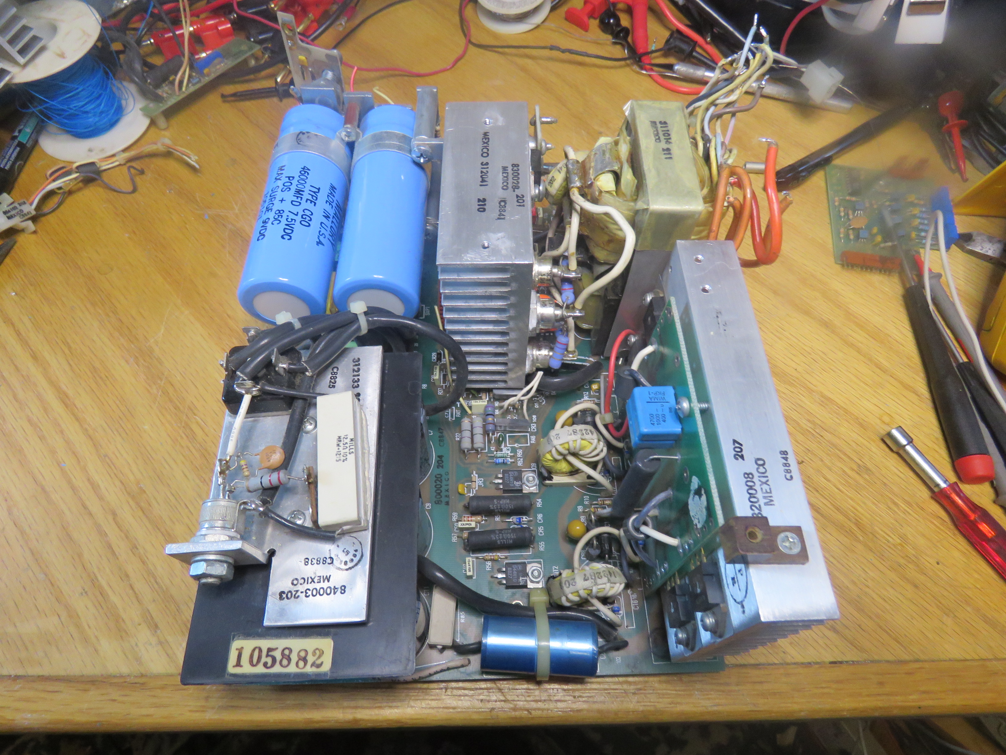
Here it is with
the top board removed. The rear heat sink is the diode bridge. Big
blue caps are the output filter, transformer is upper right. The
Half H Bridge is on the right heat sink.
Interesting magnetics. The top one is the main transformer. The
bottom one is the main 120A output inductor. The 3 wires, R/Bk/Wh
(disconnected here) are the transformer primary, the top wires are
the windings that go to the Aux board. A total of 6
isolated secondaries.
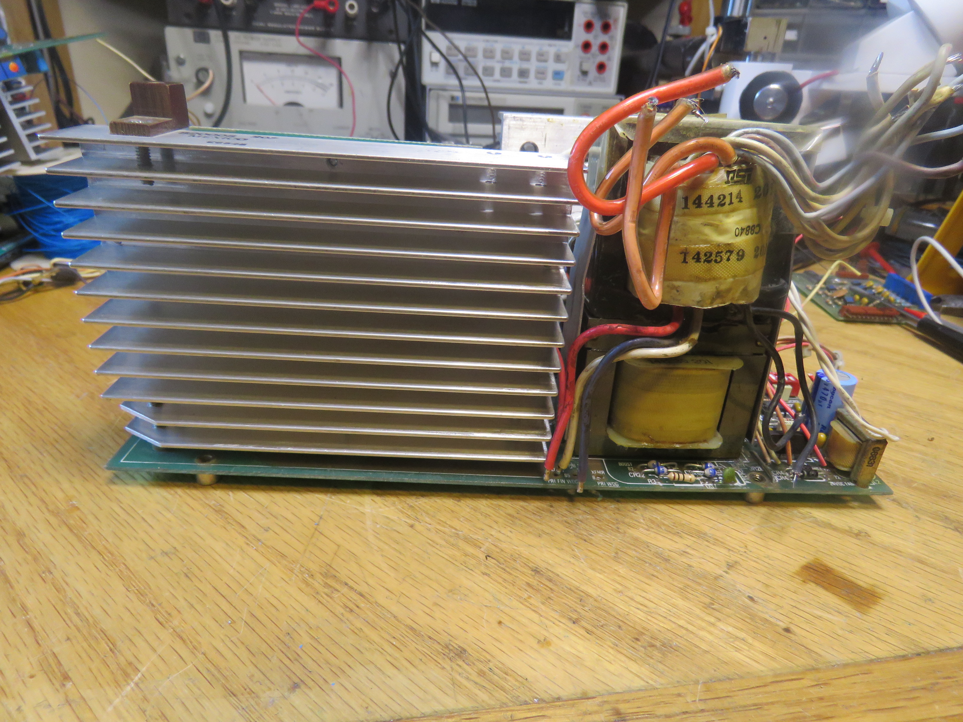
Here is the main output assembly and 120A path. From left to
right: Transformer atop inductor, Diode heat sink, output caps,
output terminals with filter board.
The
yellow toroid is the output current sense transformer.
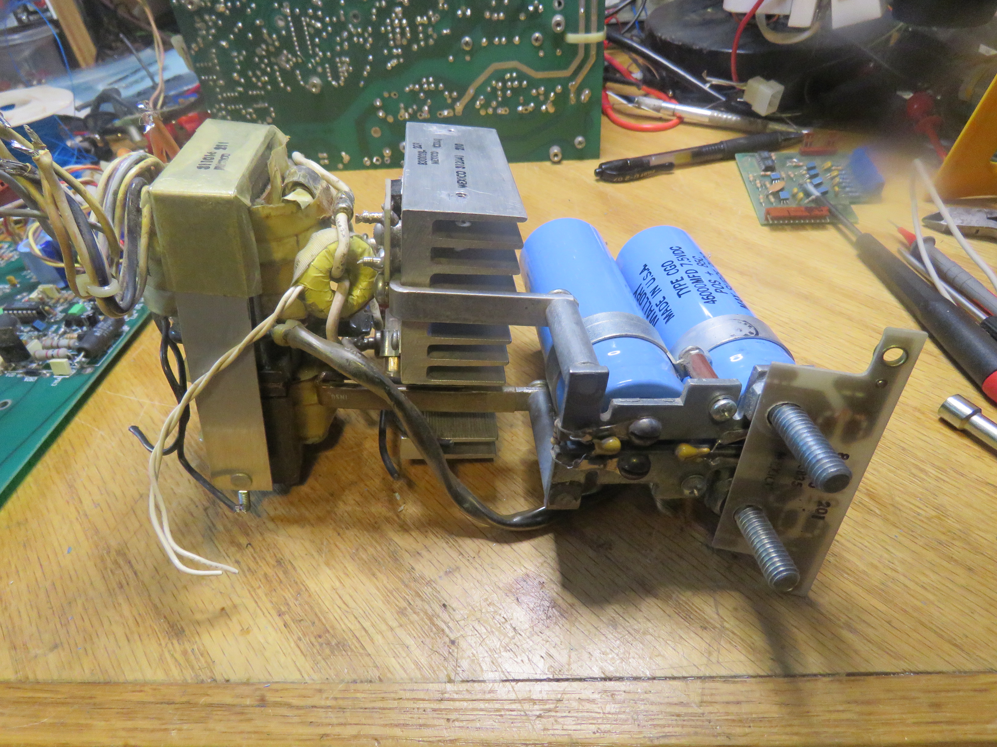
4
beefy 60A diodes, stud mounted to the heat sink, which is the
common for the 4 cathodes, and the + output of the supply. The 4
blue resistors and mostly hidden orange cap are snubbers.
The
main 120A winding of the transformer and the inductor are copper
buss bars. If you look close behind the white wire, you can see a
black blob. It's heat-shrink over the the connection from the
transformer CT buss bar and the and the inductor buss bar.
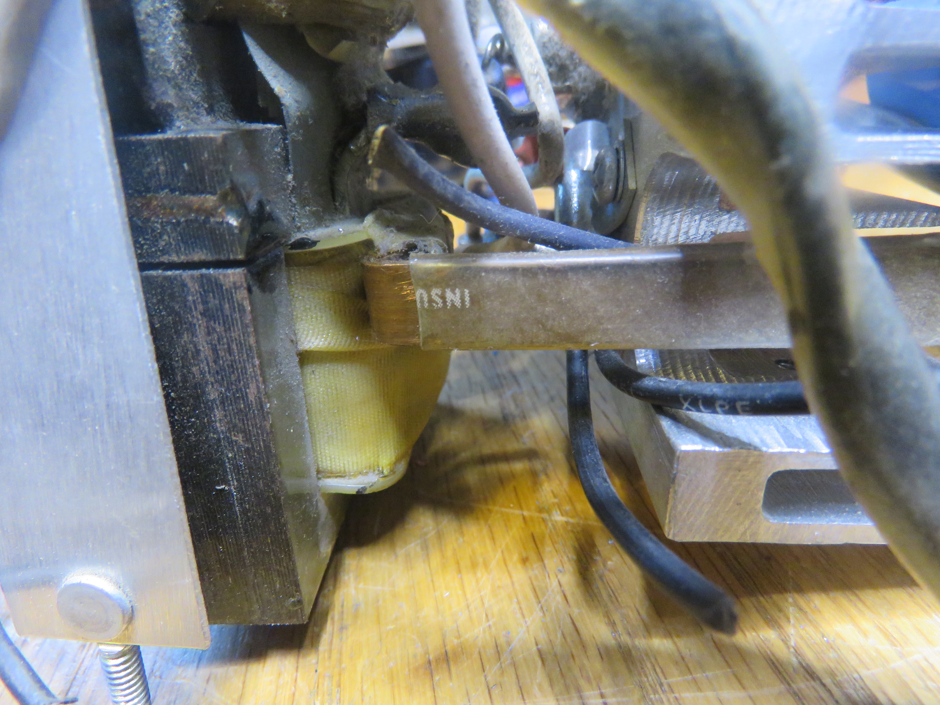
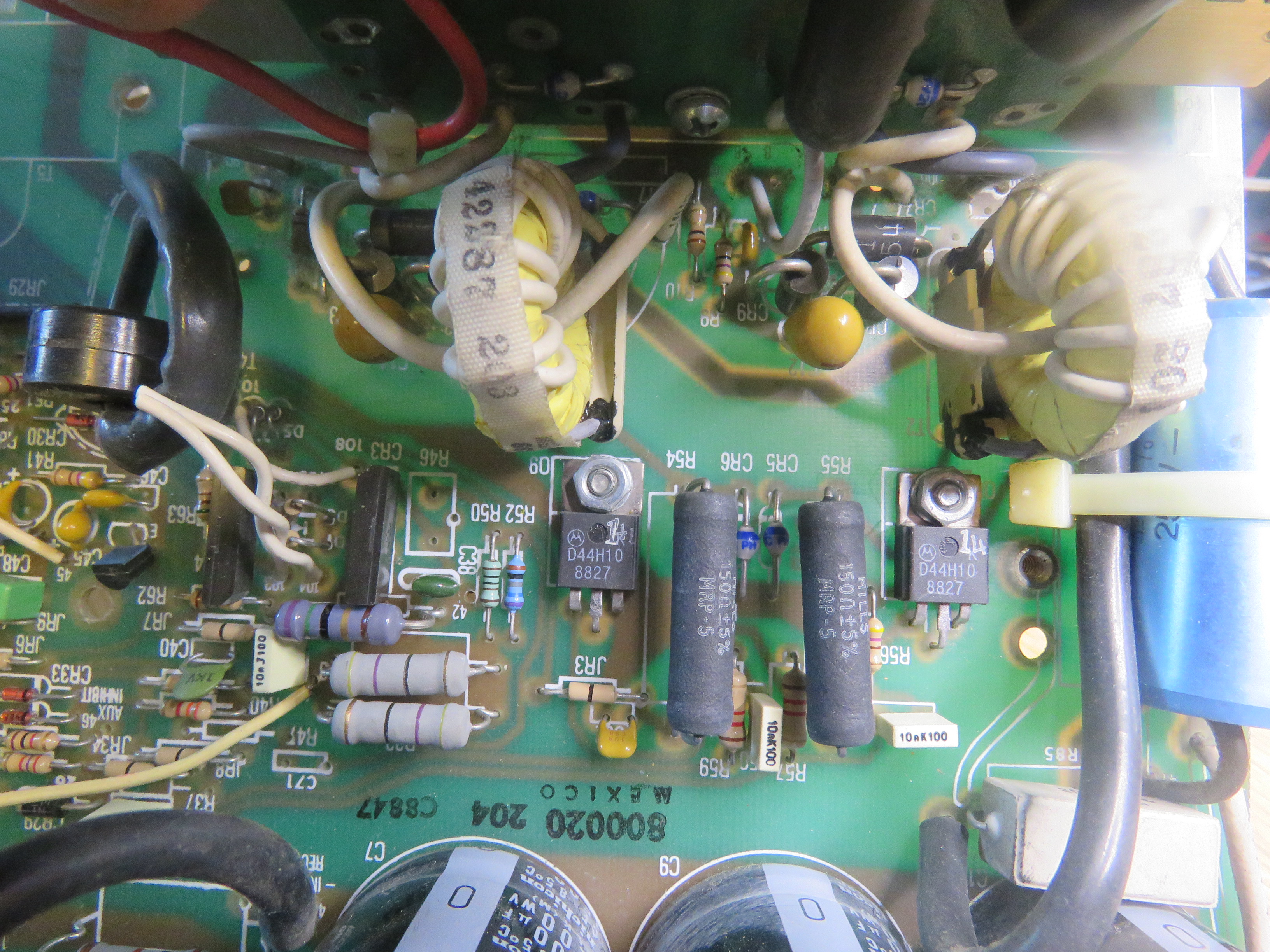
This shows one side of the main 120A secondary winding.
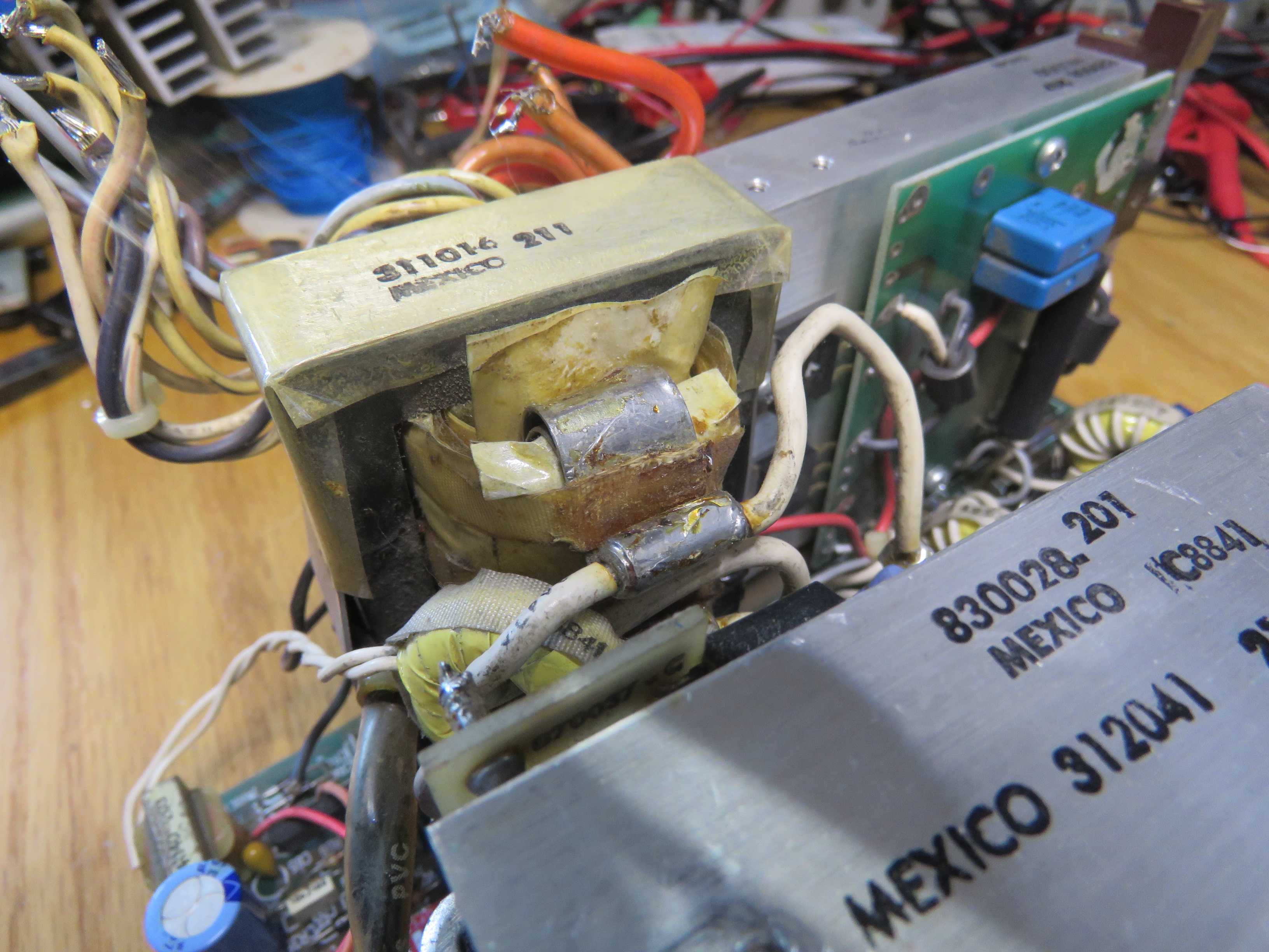
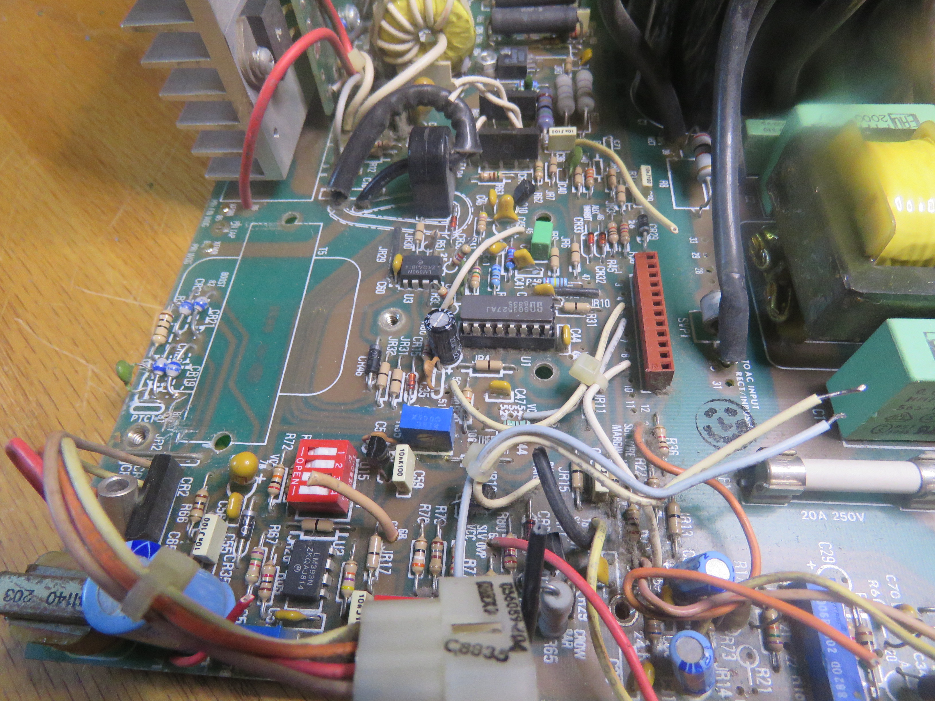
The
main board. From bottom left, CCW: AC in, fuse and filter, input
diode bridge and inrush limiter, over he 6 main caps, H-Bridge
heat sink, and a hole where the transformer goes.
Main controller area with SG3527A controller.
The
half-H bridge and its toroid Base drive transformers and driver
transistors.
Close up of the base drive circuit.
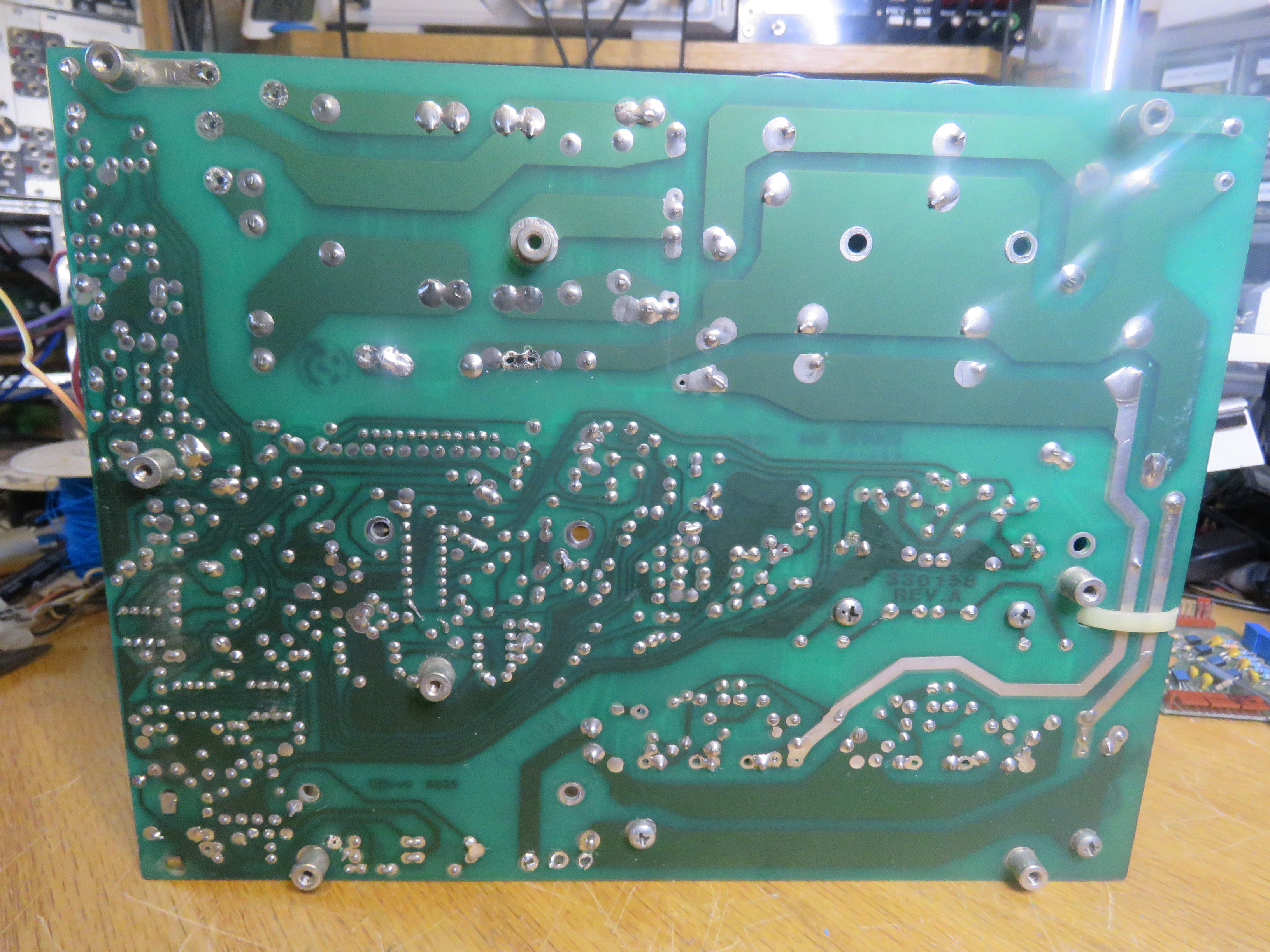
The
back of the main board. AC in and 6 main capacitors on top, H
bridge driving the transformer primary on the bottom. The rest is
control circuitry.
AC
In, rectifier, inrush limiter and 6 black filter caps. Blue output
caps and diode heat sink block the view.
Inrush limiter Triac, resistor, and AC-DC Diode Bridge
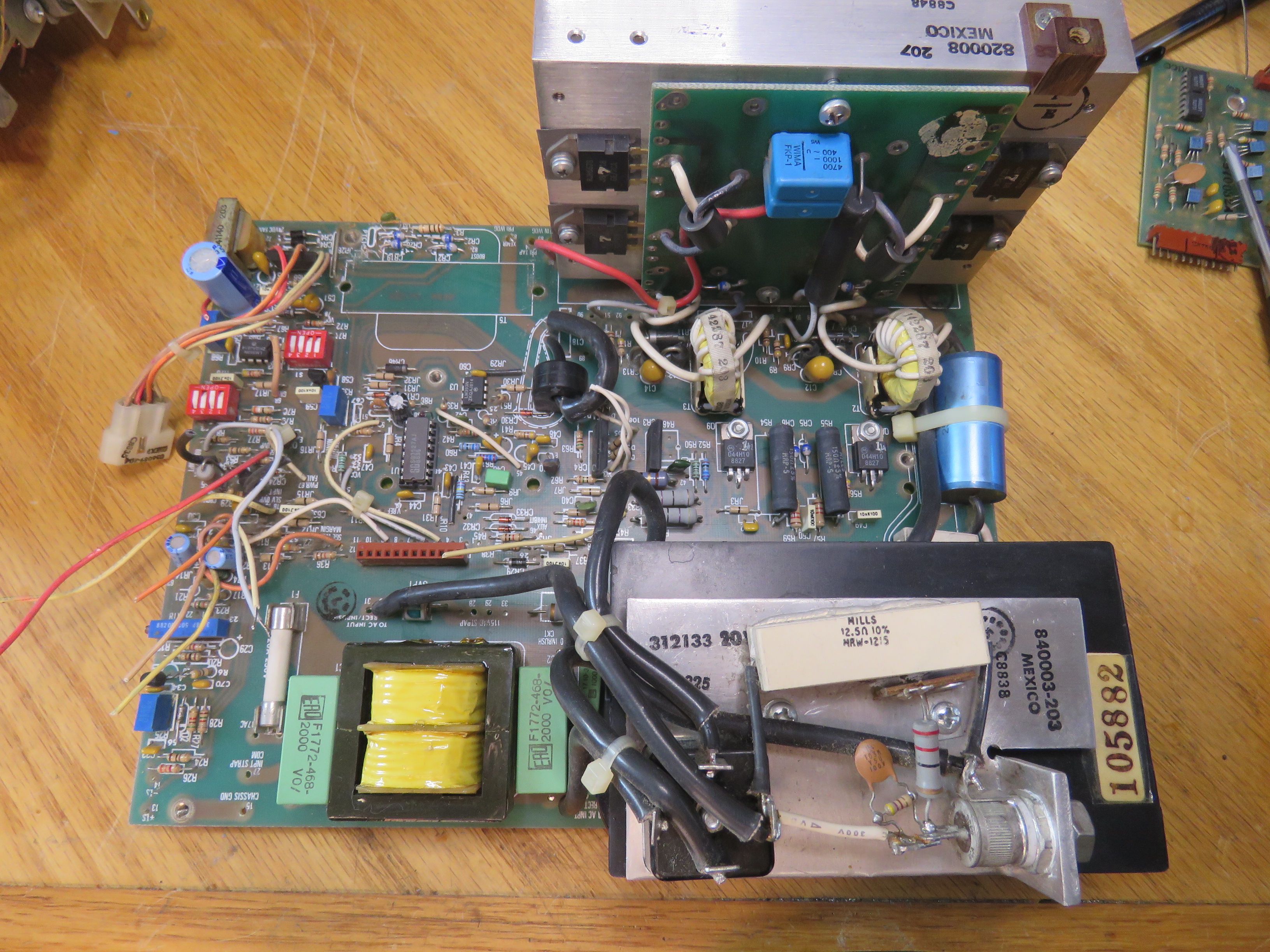
The
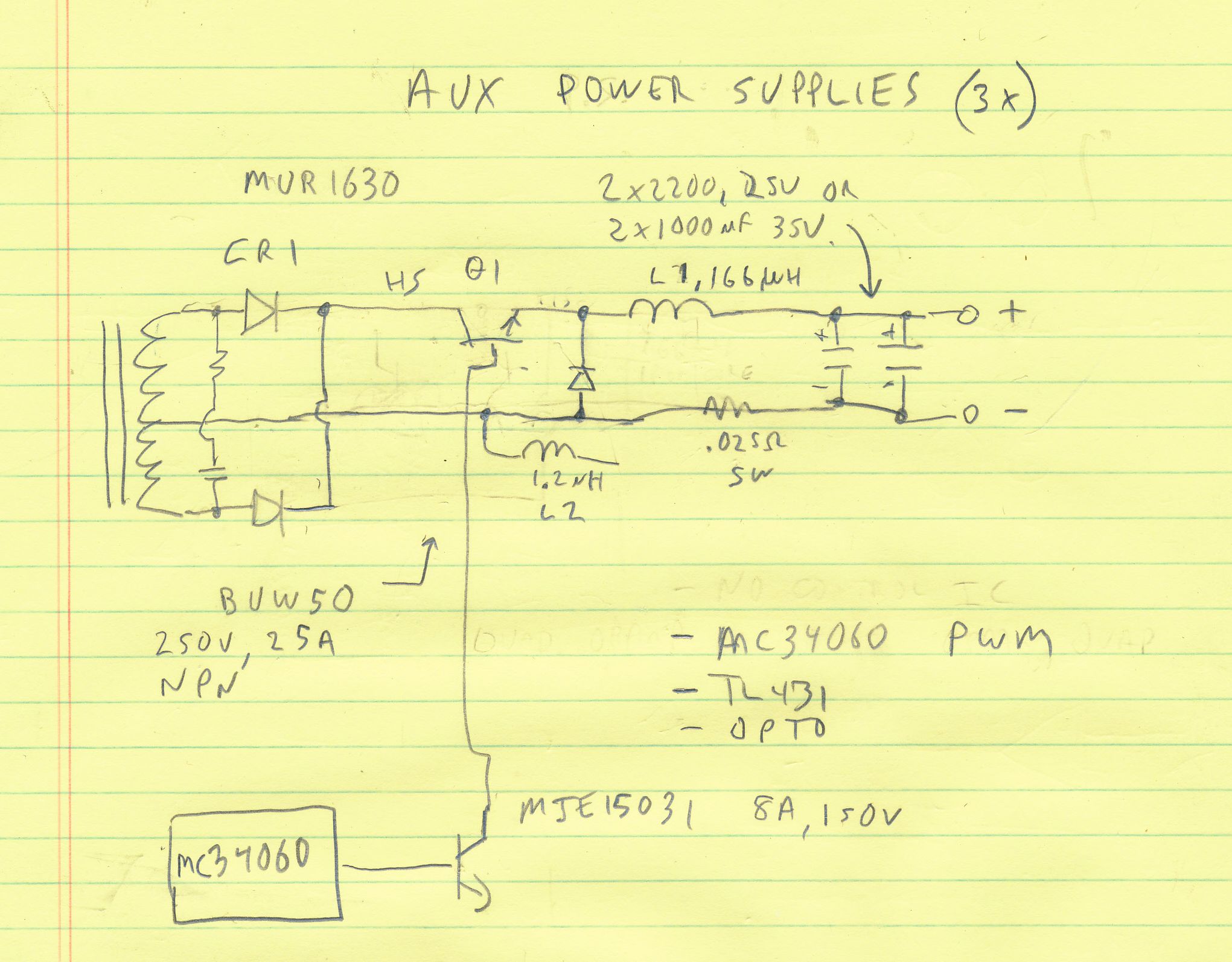
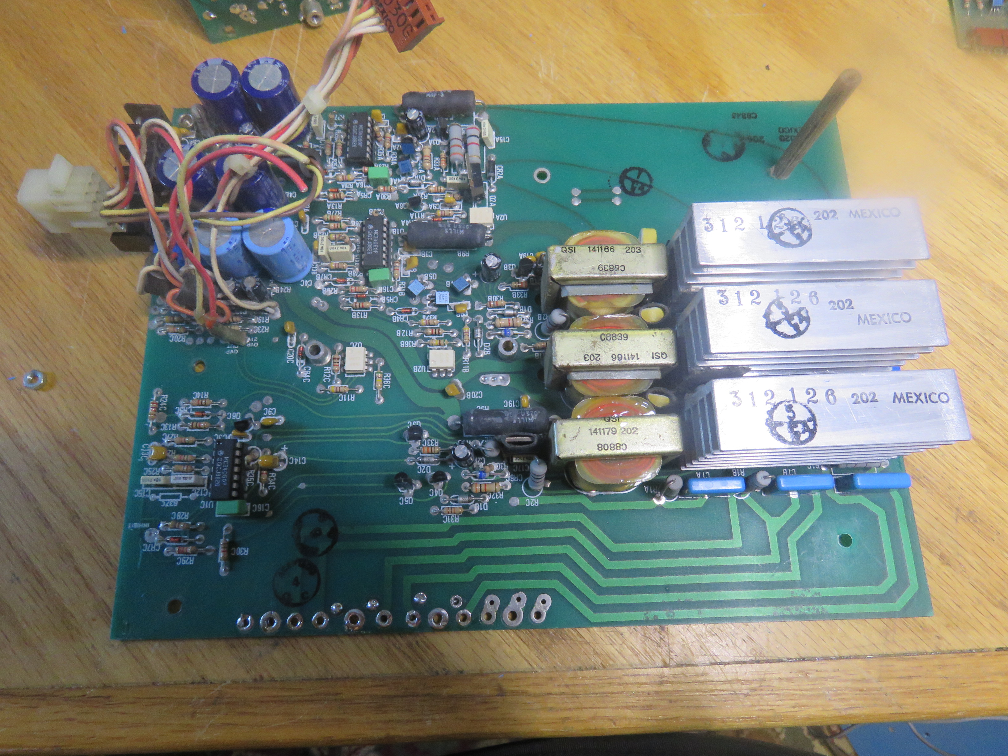
Aux board contains three isolated buck controllers for the +12,
and -12, 10A and +24V, 4A power supplies. Here is the power
path schematic for each of the of the Aux channels.
Auxilliary 3 power supply board. Main AC Transformer windings come
in on the bottom. DC out is the (hidden) barrier strip on
the top left.
The
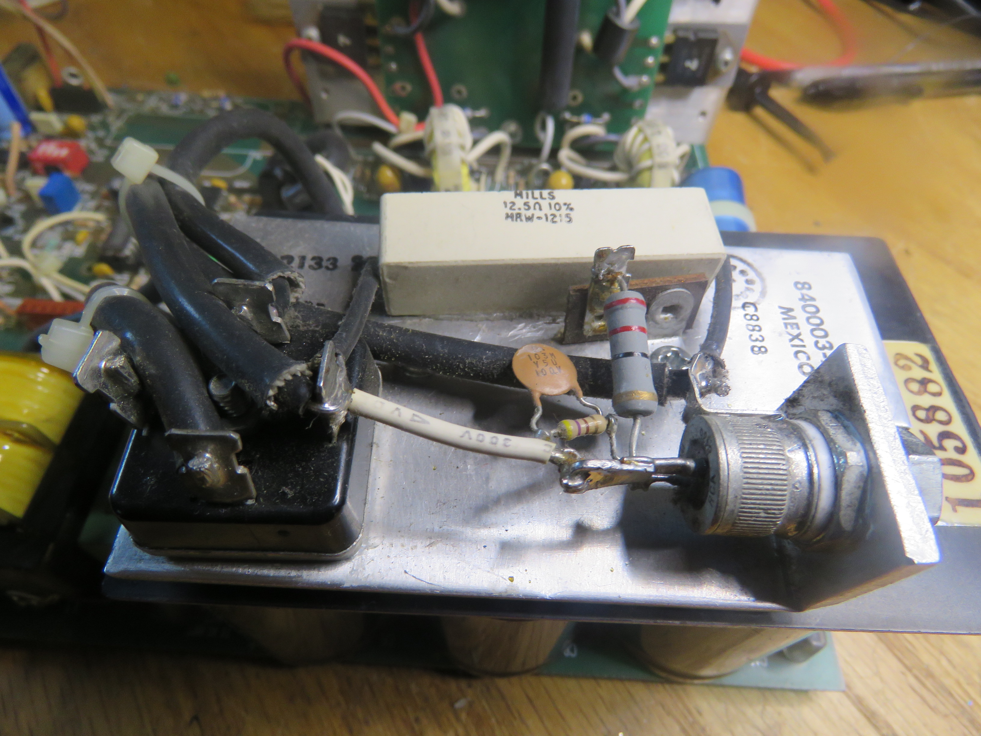
back side of Aux Board
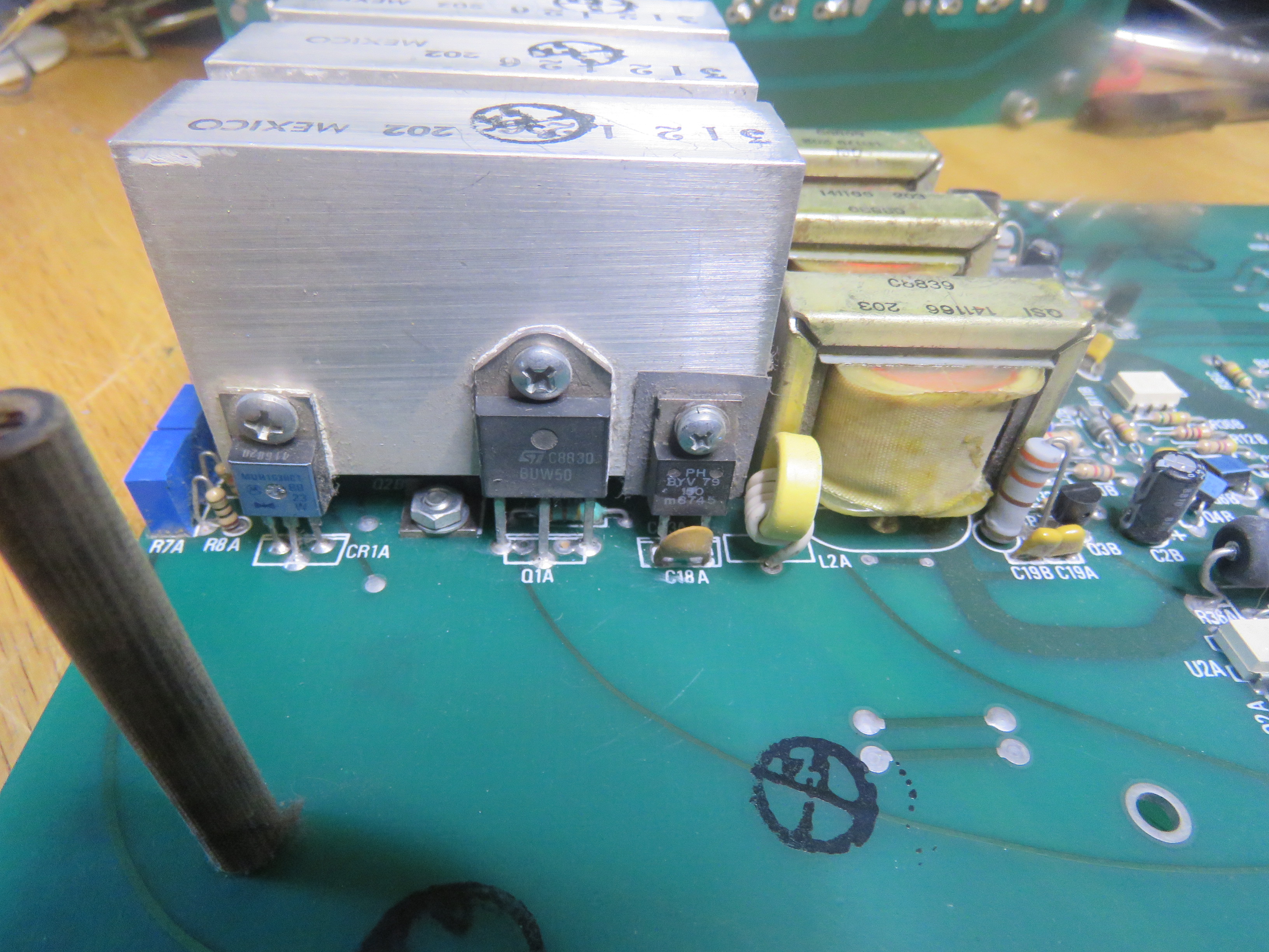
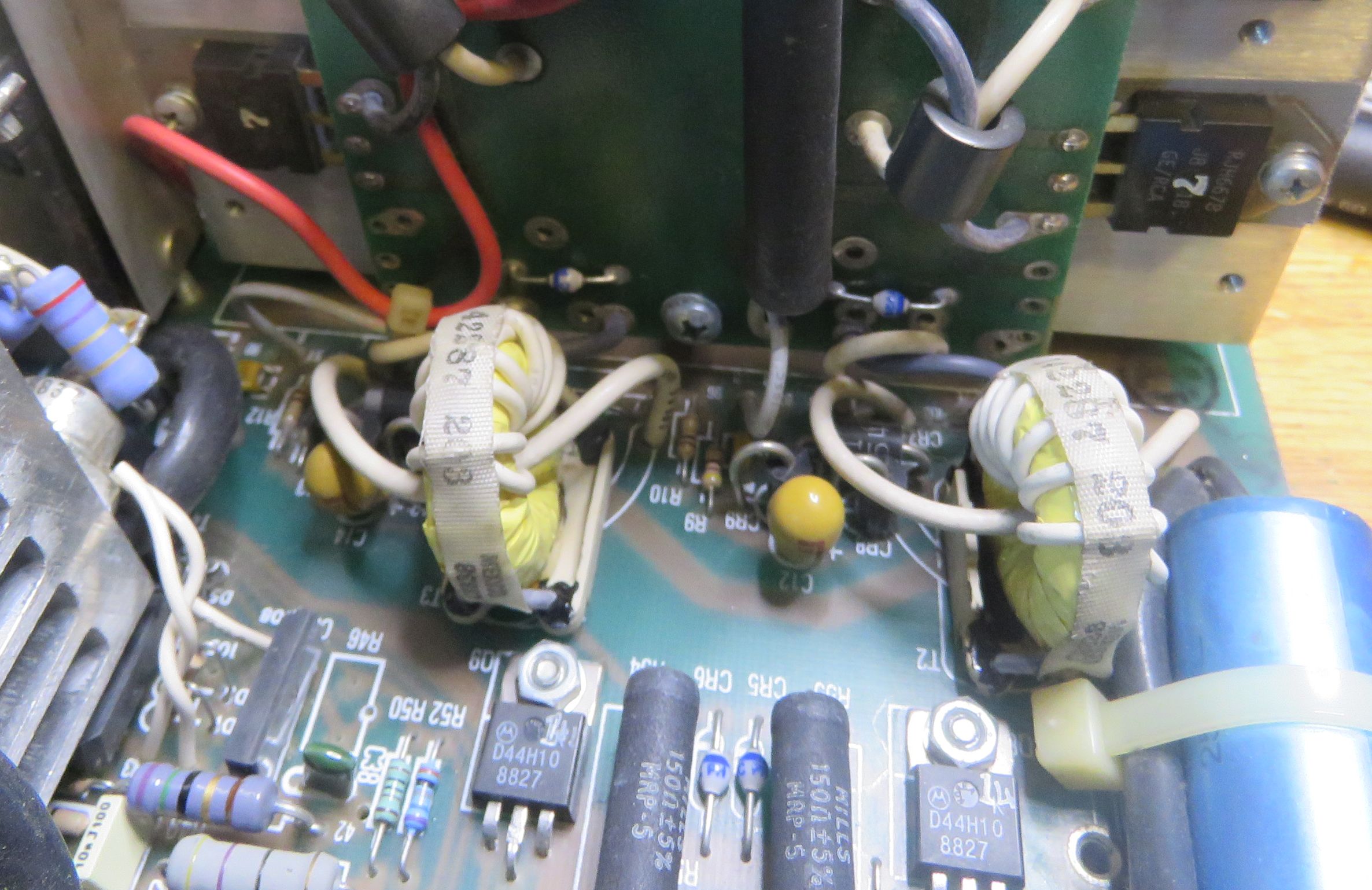
Here are the power devices for one Aux channel. The small toroid
L2A was the part that was loose in the case when I first bought
it.
Interesting
Stuff. At least I think so.
H-Bridge,
Base Drive Toroids
The H-bridge is
old school, using four RJH6678 NPN transistors. These are 400V,
15A, TO-218. The isolated base drive is from 2 toroidal
transformers, driven from two DH44H10 NPN transistors. These in
turn are driven from the main SG3527A controller IC. The toroids
need to provide about 1A of fast switched base drive to the
H-Bridge transistors. I couldn't figured out how 2 toroids with
one secondary each drive 4 high-voltage transistors. Another
mystery of these toroids is the one-turn current-sense-looking
wire running through each one.
Later, I discovered that it is not a full H-bridge, it is a half
H-Bridge. The four transistors are actually two pairs, each pair
in parallel to increase the current capability. The other side of
the transformer is driven by the common of the +/- 160V DC, via a
big film capacitor in parallel with a 200W power resistor.
Each
base drive transformer drives two transistors. Mystery solved.
Iron
Core Inductors, not Ferrite
The main 120A
inductor, and the three Aux filter inductors are laminated
iron core, not ferrites. After examining them closely, the
laminations are thinner than typical AC magnetics. Apparently thin
enough to minimize eddy currents at the 26KHz switching
frequencies. The main inductors are wound with copper buss bars.
As is the main 120A secondary of the main transformer.
The
AC common-mode choke is also iron core.
AC
Inrush Current Limiter
An AC inrush
current limiter is used to charge the six big DC capacitors
without blowing the AC fuse. It consists of a 12.5 ohm power
resistor in parallel with a big power triac. When AC power is
first applied, the triac is off, and the ac current is limited by
the 12.5 ohm resistor. Then when the main transformer starts up,
an isolated winding drives the triac gate and turns ON the triac,
allowing full AC current to flow to the diode bridge.
On
other switching power supplies, there are several other strategies
used to address this problem:
- NTC
thermistor in series , good for lower power switching supplies
and also for big AC transformers.
- Resistor
plus a relay
- Add a
PFC stage
PFC
(power factor correction) is primarily to reduce AC current
harmonics, but can also provide controlled inrush current
limiting PFC is generally required in Europe for power supplies
of > 80W. PFC reduces the current spikes and therefore AC
waveform current distortion of the power grid. The regulatory
spec is "IEC 61000-4-7 for harmonics and inter-harmonics
measurements". It specifies the maximum amount for the harmonic
content of the AC current waveform. The US and other regions are
not so restrictive. But if you intend your high-power product to
be sold in Europe, PFC is a must. For any product that draws
over 80W, you should have PFC. Not sure how cheap 200-500W PC
power supplies get around this.
Aux
Channels
Each Aux power
supply channel is a buck (step-down) regulator. It gets its input
from an isolated winding of the main transformer. I haven't
figured out if the buck converters are synchronized to the main
transformer. I suspect not. The controller for each channel
is an old school Motorola (now On-SemI) MC34060.
There is a small PCB that connects between the Aux and Main
boards. It has four TL431 references, 4 trimpots, and two ILCT6
dual opto isolators. Pretty sure it is the over-voltage detector
for the auxilliary channels.
I
was able to power up and test the two 12V Aux channels by simply
applying +24V to their input transformer connections. I applied +
40V to the other +24V supply but no output. I didn't do much
testing, just no-load. Gotta save something for later...
Low
Voltage AC transformer
A small
AC transformer was mounted to the front panel, near the fan.
This has a single center tapped primary, it can be wired
to either 120VAC or 240VAC. The 120/240 jumpering takes care of
this. The secondary is about 15VAC, so ~20V peak. This
transformer provides low voltage to the controller, the fan and
the other control circuits. The 24V fan gets about +20V so does
not run at full speed.
After
the main transformer starts up, an isolated "boost" winding and
a separate diode bridge take over and provide the low voltage DC
power. It's probably a bit more efficient that way.
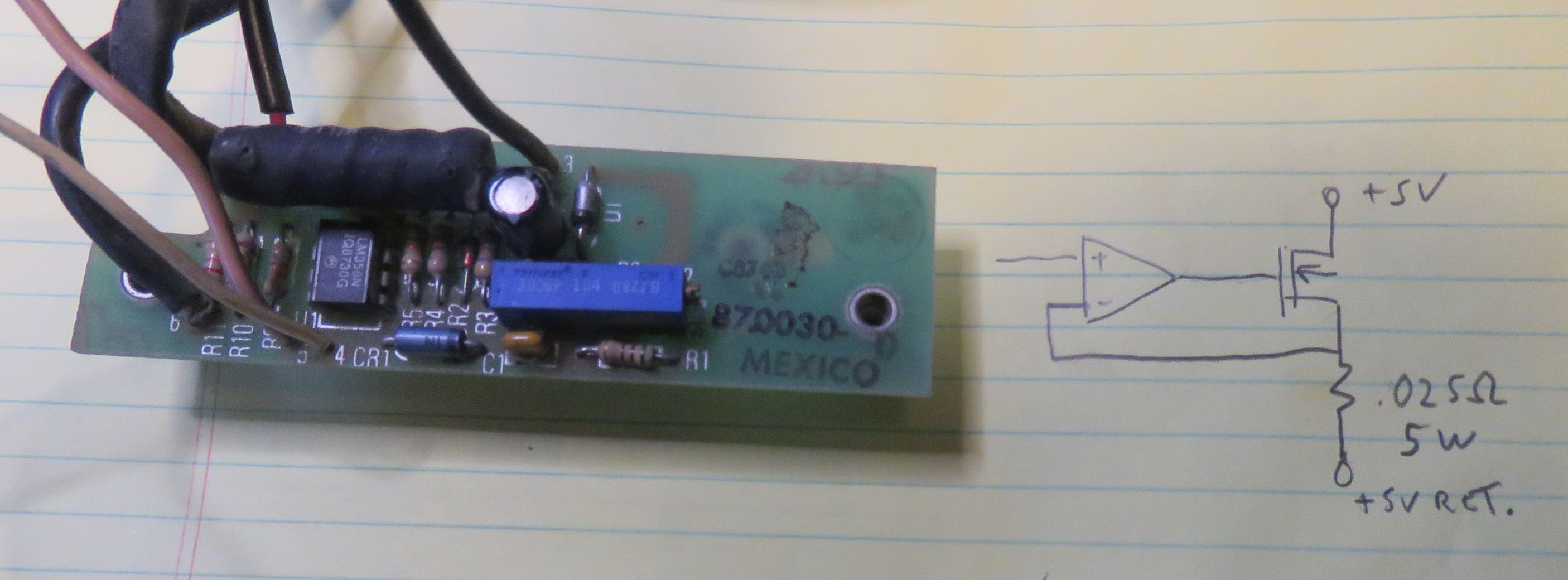
Minimum
Current Load Option Board
When we
first bought these power supplies, there was a minimum load
requirement of a few amps on the +5 supply. Without some load, the
main transformer did not have enough oomph to drive the various
Aux and other functions. Early PC power supplies also had this
requirement. Later, the design was changed to remove this
requirement. This small board, wired to a large power FET provides
about 5A of load when the +5V load current is below the minimum.
Here is a guess at the simplified circuit. The power FET is
mounted to the Diode heat sink. This makes sense for 2 reasons:
- The
drain of the TO-218 N-FET is screwed directly to the heat
sink, which is the +5V output. No heavy wire or insulation
required.
- The
circuit only operates when the power supply and thus the
output diodes, are at low current. So the extra 25W or so that
the FET dissipates does not cause extra temperature rise on
the heat sink.
The
additional wires are likely there to turn the load on and off.
Moment
of temporary insanity
As I
looked at this dissected pile of 1980s power electronics, I
couldn't help but think: "Hey, I can fix this!"
I
set about returning the main section 5V 120A power supply to
semi-operational condition. I had cut a lot of wires to separate
the assemblies, but fortunately the colored wire stubs were still
there. The PCB is labeled with many of the wire functions. These
were a big help Big help. Some of the wires that were cut or
bypassed were:
- Current-sense
transformer for secondary +5V winding: 2 white wires,
reconnected.
- Thermal
cutoff switch: 2 black wires, left disconnected. This
switch is normally open and closes at high temperature. .
- Overvoltage
control wires from Aux board: Left disconnected.
- Main
transformer secondary Boost winding to main board for low
voltage DC: Left disconnected at first
- Small
startup AC transformer for low voltage DC: replaced by a 20V
DC lab supply for now. Handy to see the current draw, since
the current actually increases when in shut-down.
- AC
Input: Switch and IEC receptacle were
added, along with 2A fuses to allow only low power operation,
AC in is hard wired to the board, AC terminal strip is
bypassed.
- Fan:
unused. I'm running this at low power only.
- 120/240VAC
wiring to the AC in barrier strip: Replaced with a jumper wire
to do 120VAC only
- Overvoltage
sense board from Aux supplies: Removed
- Switchable
5V load board that provided the minimum loading: Removed,
running with a 5A 5V 25W load resistor instead.
- Output
filter board: This provides EMI filtering for the channel.
Removed until a better ground
- Inrush
current limiter Transformer winding: Disconnected, running
with current limiter only for now.
- Aux
power supplies board: Removed, transformer windings taped
off.
With no
load, the unit would charge the output caps to 5V and then shut
down. It would recover after a while, and then do the same
thing. I added the 1 Ohm (5A, 25W) load, and it did pretty much
the same thing, but wold not recover until all power was
completely removed.
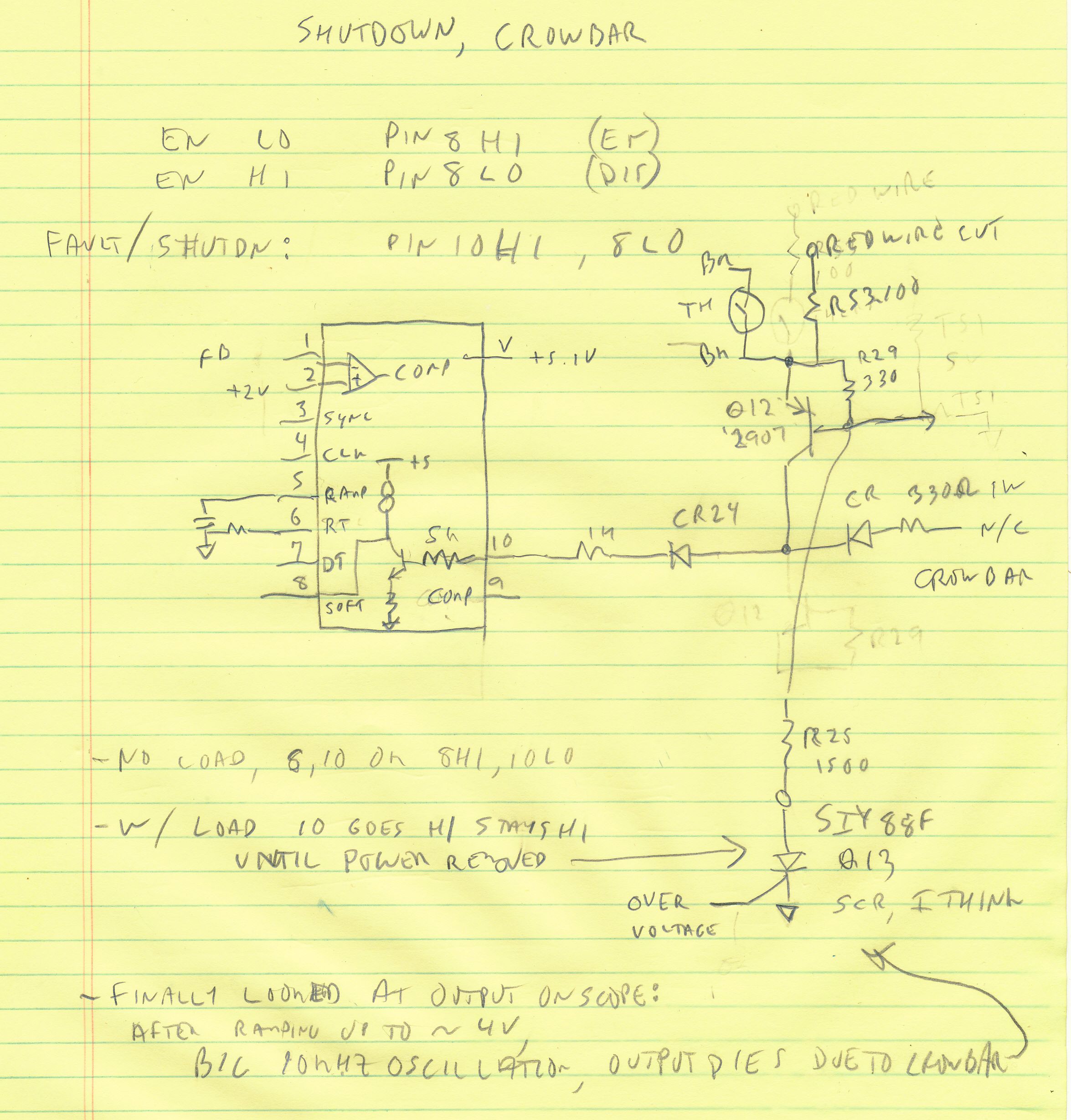
Understanding
that there are many conditions that could cause a shutdown, I
set about isolating which one(s) were causing it.
- Main
Power Supply over-voltage
- One
of the 3 Aux supplies over--voltage
- Main
Supply over-current
- Aux
supplies over-current
- Over
temperature on the diode heat sink
SG3527
pin 8 is the SOFT START pin. Pulling it low causes shutdown. Pin
10 is the SHUTDOWN pin. Applying +5V causes shutdown. Pin 10 was
the one causing the shutdown. I traced the circuitry via a
PNP transistor to an unknown part. This TO92 package was labeled
SIY 88F. Couldn't find it on Google. Normally one pin was 10V
and the others low voltage. Kind of like an NPN transistor. When
it shut down, the input were still 0, but the output went
low. Huh? Turns out it is a small SCR that provided the
overvoltage Crowbar function. An SCR is used here because it
stays latched and shuts down the system until power is removed.
I disabled the output of it, and the supply went into a bizzare
screeching mode, with the 5V output only 2.5V. I reconnected it
quickly.
Here is
the shutdown circuit.
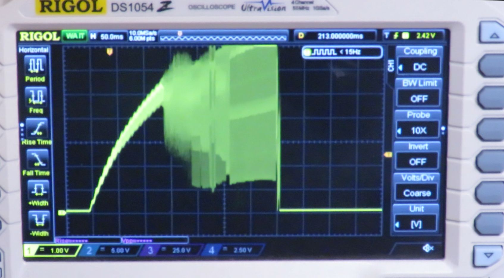
"When
you get strange DC results, turn on the oscilloscope." I
triggered the 'scope on the +5V rising. Strangely, the output
would ramp up to about 5V, then increase to +7V. The output had
about 6V p-p of sawtooth at the switching frequency, for
about 200mS. Then it would shut down due to triggering the
over-voltage circuit crowbar. Here is the scope shot of
the +5V coming up. 6V p-p of 26KHz crud! This is not a
happy power supply.
For
about 3 seconds, I wondered how those giant 46,000uF caps could
have so much high frequency across them. Duh, both capacitors
were dead! I jumpered a 1,000uF 35V cap across the output
terminals, and the output quieted. I removed them, and on my LCR
meter they both measured under 1uF. Fortunately my junk bin had
some large caps. I installed a 12,000uF 25V and 18,000uF
25V, and the supply came to life, outputting nice stable +5V.
30,000uF is not 92.000uF, but it's way better than 2uF. New caps
are about $20-30 each, and I ain't paying that. I'll see how far
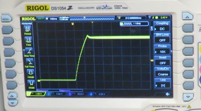
these mismatched old ones get.
The 5V
output power-on with new caps installed. Sweet!
So
you're probably asking "Why didn't this dummy suspect the output
caps at first?". Well I did, but they looked good, no bulges or
leakage, and seemed to hold a charge. Also there are 2 in
parallel, so they'd both have to be real bad to cause the power
supply to not work at all. Yep, they were. They could not be
measured in-circuit easily with an LCR meter. Since they were
after diodes, I could have charged them with an external power
supply or my trusty DIY-SMU, to see if they held a charge or were
excessively leaky. SMU at 10mA range should take T = C * V / I,
so T = 90,000e-6 * 5V / 10mA = 45 seconds to charge or discharge
5V. Easy test, hindsight is 20/20. A 5V power supply through
a 500 ohm resistor would also do it.
I
have no excuse for not 'scoping the output at first. Better late
than never. Hopefully others will learn from my mistake.
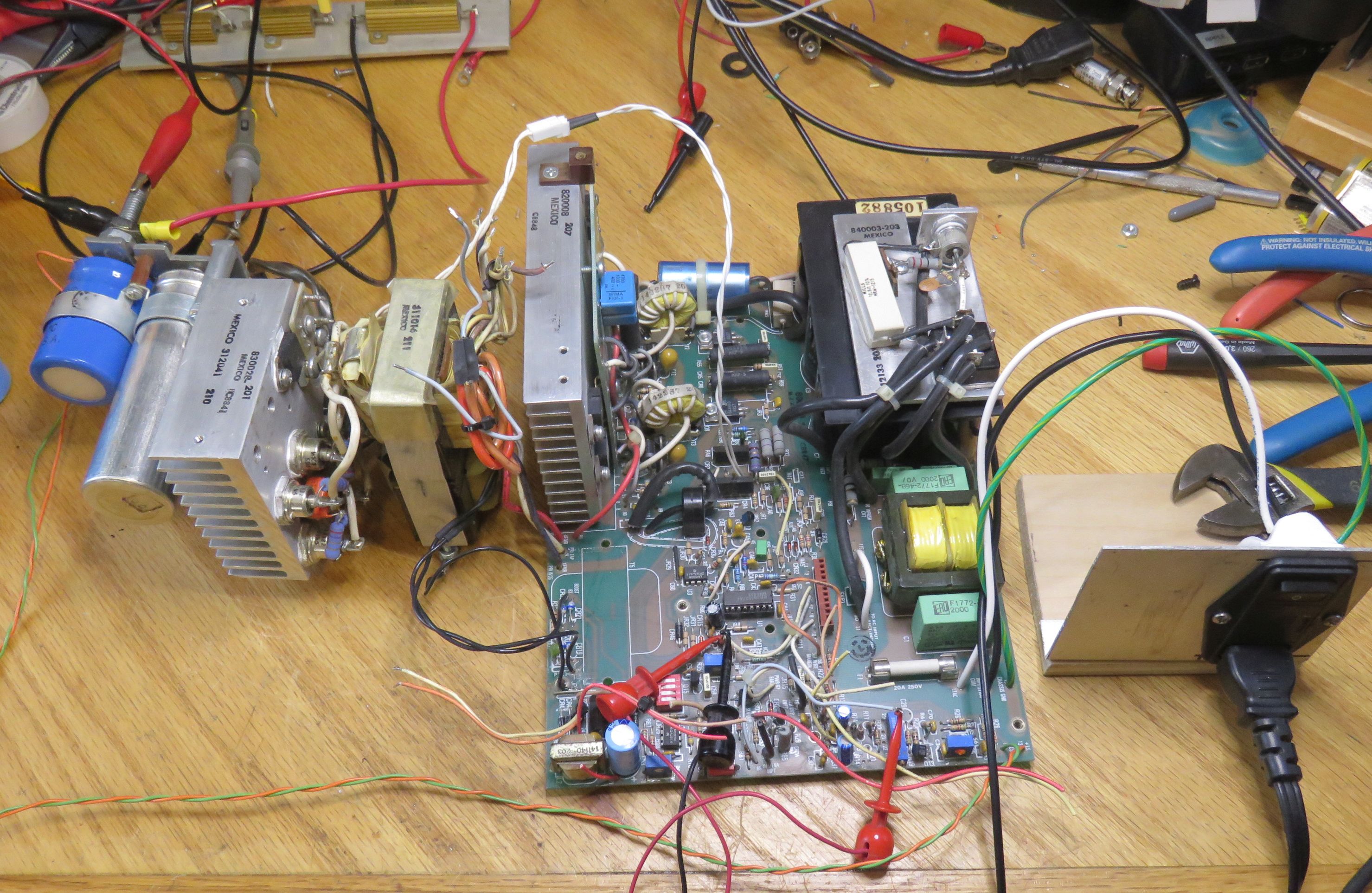
Frankenstein
power supply. It's Alive!!
Here are the
main board, main transformer and main output path set up to try
and get it working. Note the mismatched output caps on the left.
High(er)
Current Test
I operated
the supply with a 5A minimum load and a 10 to 20A load from my DIY
E-load. 20A plus the 5A minimum load is a 25A, so a 125 watt load.
Upon increasing the load to 25A, the power supply drew about 200W
of AC power. The 12.5 ohm resistor in series with the AC line
became very hot. This is because the Triac had not been turned on.
I connected the Triac to the Triac Gate winding of the
transformer, and the 12.5 ohm resistor operated at a cool
temperature. But after an AC power cycle, the 2A 20mm fuses in the
AC line blew. I replaced these with 6.3A fuses. These were the
highest value 20mm fuses at my local hardware store. To prevent
blowing more $4 fuses, I temporarily operated the supply from a
variac until I was sure it could start up and operate at 25A. If I want to
continue using this at high currents, I would use fuse(s) larger
than 20mm, about 10-15A, maybe slow-blow
Interestingly, when it does operate with the inrush triac,
there is a 120Hz buzzing noise from the AC input section. I traced
this noise to the AC filter common-mode choke. The varnish that
holds the choke's iron core laminations together may have dried,
causing the buzzing. Or the noise may have always been there, but
was masked by the board being in a box that was inside another
box, and the fan noise from the power supply and system fans.
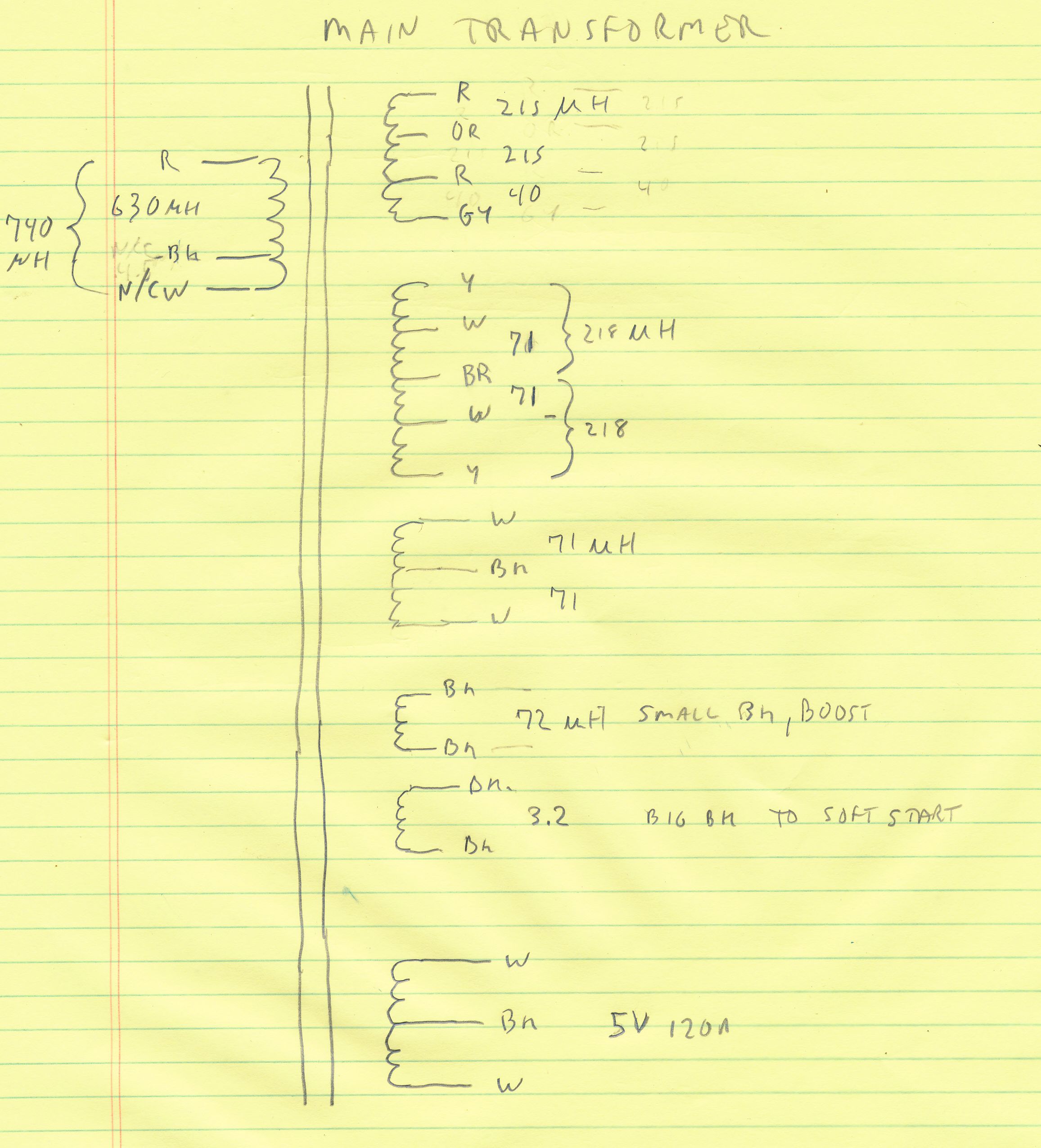
Main
Transformer
This is a
detailed schematic for the main switching transformer. The primary
has 2 taps, the white wire tap is unused. There are 6
secondaries. You can calculate the turns ratios from the
inductances if you are interested. N2/N1 = sqrt(L2/L1).
- The
main one, 5V at 120A, center-tapped, wound with copper strap. I measured
4.6uH per side
- 3
auxiliary center-tapped secondaries with various voltage taps
- Boost
winding to power the electronics after startup
- Soft
start disable winding turns on the AC triac
What to
do with this thing
As I've
stated, I have no use at all for a 5V 120A power supply. However I
do have a use for a system that can test transformers, inductors,
other switching power supply components, etc.
If you stand back and squint, you'll see a similar architecture
used in old PC power supplies. The old ones use a similar
Half-bridge and are quite hackable. My advice. If you have an old
half-bridge PC supply, particularly one that uses a TL494, hang
onto it.
This supply has many things in common with old PC supplies. Here
is a typical old-school PC 200W Power supply.
It is
kind-of an old-school PC power supply on steroids:
- AC
Line Filter
- 120/240
VAC jumper / switch
- Inrush
current limiter
- Full
wave diode bridge
- Bulk
caps are +/- 160V using 2 capacitors
- Half-bridge,
2 NPNs
- Some
PCs are FET
- Single
primary winding
- ~1uF
Film cap from center of bulk caps to main primary
- Output
inductor for main channel
- PC
has one multi-winding inductor for all channels
- Multiple
secondaries
- Qualidyne
has isolated Aux supplies
- PCs
have common ground for all outputs
- Base
Drive transformer(s) for base (Gate) drive
- Grounded
side control chip, push-pull
- SG3527
for this
- TL494
for most PCs
- Direct
V sense, not isolated TL431 + Opto
- Bootstrap
low voltage supply for initial power-up
- Boost
supply after power-up for efficiency
- Can
be AC or switching transformer
- Typically
a few watts
- Enable
signal to turn on supply
- Power
Good output
- Overvoltage
protection
- Snubbers
on transformer primary and at least one secondary
- ....
Note that
modern PC power supplies (> ~y2000) are smaller, and most use
more advanced configurations. These are not be as hacker-friendly
as the older ones. Fancier transformers, more integrated. Here is
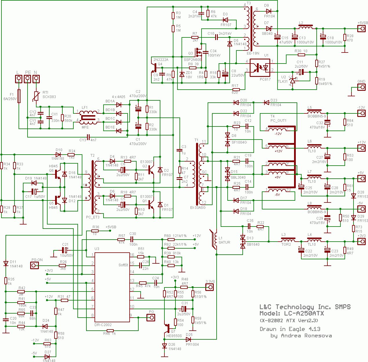
a schematic of a more modern supply. https://www.smpspowersupply.com/atx-power-supply.html
They also use a saturable reactor to regulate the
3.3V. Old technology in a new application.
- Single
bulk HiV cap, 450V
- Probably
a single FET, forward converter.
- Multiple
primaries on the transformer.
- Auto
120/240 switching
- More
+12V current, less +5V and +3.3V
Analysis
of half-bridge PC power supply
I
discovered an interesting winding on halfbridge power supplies.
It's on most PC power supplies, but in addition I found it on
the 1980s Qualidine power supply that I did a YouTube video on.
In that case it was very distinct. It's a heavy wire that's run
through the center of the toroid base drive transformers as if
it were a current sense. But why would a current sense be on a
base Drive transformer? I've seen a few theories about what this
does. One theory is that it self oscillates the Transformer but
that doesn't seem to be the case.
Here are
the two base drive toroids on the Qualidyne. There are three
windings on each one:
- Primary
winding, driven by the transistors
- Secondary
winding, about 7 turns of medium white wire
- 1
turn of heavy white wire. through the middle.
And here
is a PC power supply schematic similar to the one I have. Note
that the base drive transformer T2 secondary has an extra tap on
one of the windings, pins 1 and 6. It is wired in series with
the main transformer primary. Similar to what is happening
on the Qualidyne.
I'm
guessing that it's about a one turn winding due to the very
low inductance. And that it serves the same purpose as the
heavy wire run through the center of the Qualidyne base drive
toroids. On the PC supply, I measured the base drive voltage
on the primary, while varying the load on the power supply,
and the base drive voltage varies
considerably as a function of the power supply current load.
At low currents the drive is low and it high currents the
drive is high.I measured the inductance of one
PC transformer, similar to the schematic below.
- Primary:
2930uH per side (9-18, 18-8)
- Secondaries
230uH (5-6, 3-2)
- Tap:
1.2uH (6-1)
- Primary
to Secondary turns ratio is sqrt( 2930 / 230 ) = 3.57
- Primary
to Current tap ratio is sqrt( 230 / 1.2 ) = 13.8
So if
the current tap is 1T (turn), there are about 14T on each
secondary and 50T on each primary side.
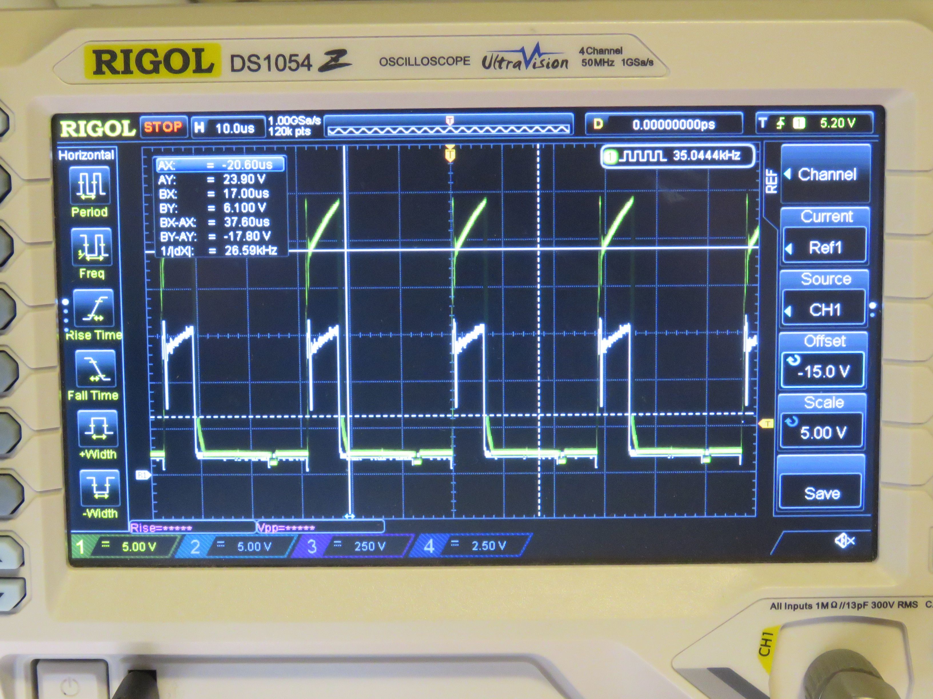
Here is the base drive waveform on one side of the primary. The
lower white trace is with a 12V, 1A load (12W) and the yellow trace
is at 7A (84W). It increases from about 13V to about 25V. The
significant increase in drive with load is due to the 1T current
sense winding. The center tap is driven by a 1.5K resistor, so is is
not driven hard. This allows the current sense winding to change the
drive voltage. Wish I had a good current probe to measure the actual
primary.
Analysis for the base drive.
The output pulses of the controller are open drain or collector.
Both are normally off, and pulse low. They are pulled high to about
+15V by the 1K/1K pull-up resistors. (my power supply uses 2.7K's to
+15V. These active low pulses drive the NPN transistor bases. The
common-emitters are biased positive with ether one or two diodes to
ground, plus a bypass capacitor. The schematic above shows one
diode, my power supply has 2 diodes. This is probably so that when
the controller outputs pull low (to GND) the transistor bases are
pulled below the emitters, for faster turn-off. You might
think that the two half's of the transformer are driven low
alternately, but no! The transistors are both ON normally and are
turned OFF by the pulses. So the transformer pulses are positive:
common emitter stages invert. The center tap is driven by a 1.5K
resistor pulled up to +15V. So without pulses, and with both
transistors ON and saturated, the center tap (CT) is pulled low,
close to the emitter voltage, 1-2 diode drops. There is about 10mA
bias current flowing through the CT from the 1.5K resistor. Then
when each side pulses, its transistor turns OFF due to the 10mA bias
current, applies a positive 10mA current pulse to the
transformer. The voltage is limited by the Output transistor base
load on the secondary So the transformer is basically in current
mode. Its 4:1 turns ratio applies about 10mA * 4 = 40mA to the base
drive. DC balance is maintained by the other side doing the
same to its winding.
The fact that it is i current mode allows the transformer to have
the additional current sense winding: 1 turn that senses the main
transformer primary current. At low currents, it does little. At
higher currents, it causes the increase in base drive.
BTW, this extra winding is only used with Bipolar power transistors.
Modern power supplies with FETs do not have this mystery winding.
And Gate-drive transformers are typically about 1:1 turns ratio. The
drive circuit typically outputs 12V pulses, and the FET gates want
to see 12V pulses. so 1:1 transformers.
Back to Dave's Home Page
Last updated 1/6/2024