DIY
SMU: Source Measure Unit Page 3: Board Bringup
The Schematics, PCB
files, and BOM are here
Page 1: the Analog part
Page 2: the Digital part
Page 4: New Case, SCPI, Testing
EEVBlog Forum Page
Youtube
Channel
Day 1: Initial build and bringup, Amp board
The PC boards and parts were ordered while I was
away on summer vacation. When I returned, there was work to do. I
started by loading the high voltage Amplifier board and powering
it up with the 240VCT medical isolation transformer. I use
an old variac to power it up, slowly increasing the voltage. The
variac is plugged into an AC power meter so I can see if something
is using too much power. I started by loading the +/- 170V and +/-
15V parts. I'm pleased to say that my capacitor voltage-drop
circuit from 120VAC to +/- 15V works as intended. Spice simulation
helped with this circuit.
When these supplies powered up OK, I installed all the amplifier
components except for the 6 output transistors. Made sure the FET
bias resistors all measure OK. The measurements are not perfect
since the ~1 Megohm circuits are being measured with a 10Megohm
DMM. Then I installed the 6 power transistors and fed in a control
voltage. This part of the amplifier runs open-loop, and without a
load resistor, the gain is very high. It took only about +/- 50mV
to cause the output to swing to the rails. I tried a 10K load
(100V at 10mA) and this reduced the gain, but was careful to keep
the current low since no heat sink was installed yet.
Day 2: Main board build and initial bringup
When I was satisfied that the amp was working, I
built up the main board. I began by loading with the +/- 15V and
+5V supplies, then the +/- 2.50V references. Digikey sent me the
wrong ADR431 reference, but fortunately I had some old
LT1019-2.5's that I could use. The supplies and references came up
fast. I use a 12V lab supply to provide the raw +12V so I can
monitor the supply current every time I add more circuitry.
I decided to get force-voltage working first, so I loaded the
parts that this needs. I decided to use only the 1mA current range
to begin with since 1mA is a safe current and would work with no
heat sink installed. I would not load the clamp current
control circuit. This was pretty simple. I could install nearly
every discrete component and just not install various
op-amps. I also decided to debug the main board without any
CPU or software. This meant that I needed to control the Force DAC
externally, and wold hard-wire the Clamp DACs for now. The initial
setup:
- Do not install the DAC, ADC and Control
registers
- Drive the force DAC externally
- Jumper the I range to 1mA
- Jumper the FV/FI switch to FV
- Bypass the output and sense relays to be ON
and Local sense.
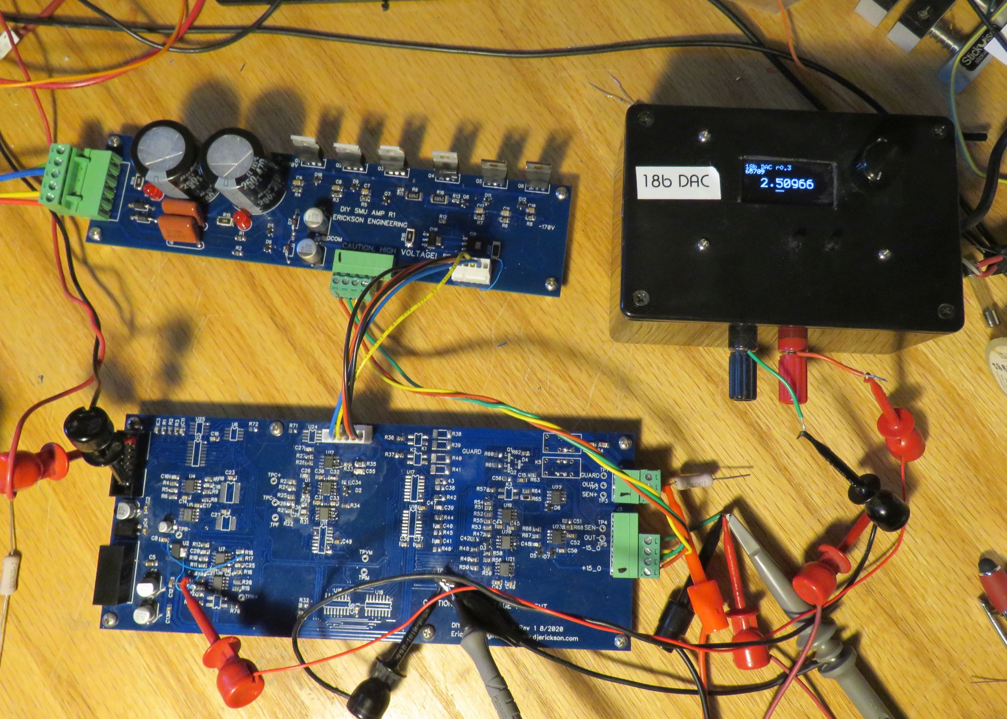
To control the force DAC voltage. I use my 18 bit DAC box. It
outputs 0 to 10V with 18bit resolution, so does a nice job of
simulating a 0 to 5V DAC. Setting it to 2.500v, the center of
the 5V DAC range causes the SMU to output 0.0V. The
un-calibrated error is under 10mV on the +/- 150V range, nice! I
ran the +/- 170) V supplies at about +/- 60V to start with. The
few times I turned the +/- 170V supplies up all the way, the
output range is about +/- 150V.
I made 2 mistakes on day 2, the first amp build,
and flames resulted! I did not add the
current limiting transistors to the amp board. And one of the 2Meg
divider resistors had an un-soldered pin. After working for a few
hours, all 6 of the output transistors
shorted out, taking the 25 ohm resistors, a couple of the 1M/2M
resistors and the driver transistors with them. Also the driver opamp on the amp board
went. After replacing all these parts, I haven't had a
meltdown now for 2 days. Lesson learned, check the soldering
carefully on the amp board before applying high voltage!
Note: This was two months ago and in the subsequent bringup and
testing, I have not had any failures with the system since. Knock
on FR4.
I also found that without the current clamps running, the voltage
across the current shunt could increase beyond it's normal 5V to
> +/- 15V. When this happens the + Sense buffer amplifier
saturates to -15V and the measure voltage can drop to 0V. This
causes the loop to constantly increase the voltage. causing output
saturation. So latch up results. It can be corrected by powering
down or by changing the output DAC polarity. I noticed that the
'236 uses a +/- 30V bootstrap amp for its + Sense amp, probably to
eliminate this issue. But I thought since I use +/-5V shunts and
not +/-10V, I could get away with +/- 15V instead of +/- 30V.
Turns out you can, as long as the clamp circuits are working
properly. After I got the clamps working, no more latchups.
Day 3: Basic Current Clamps
I installed the parts for the current clamps, and
they work well. I hardwired the Clamp DAC voltages to +5V and GND
to set the upper and lower limits to their full scale limits
without the DACs installed. With a 10K 1% resistor as a load, the
1mA clamps work.
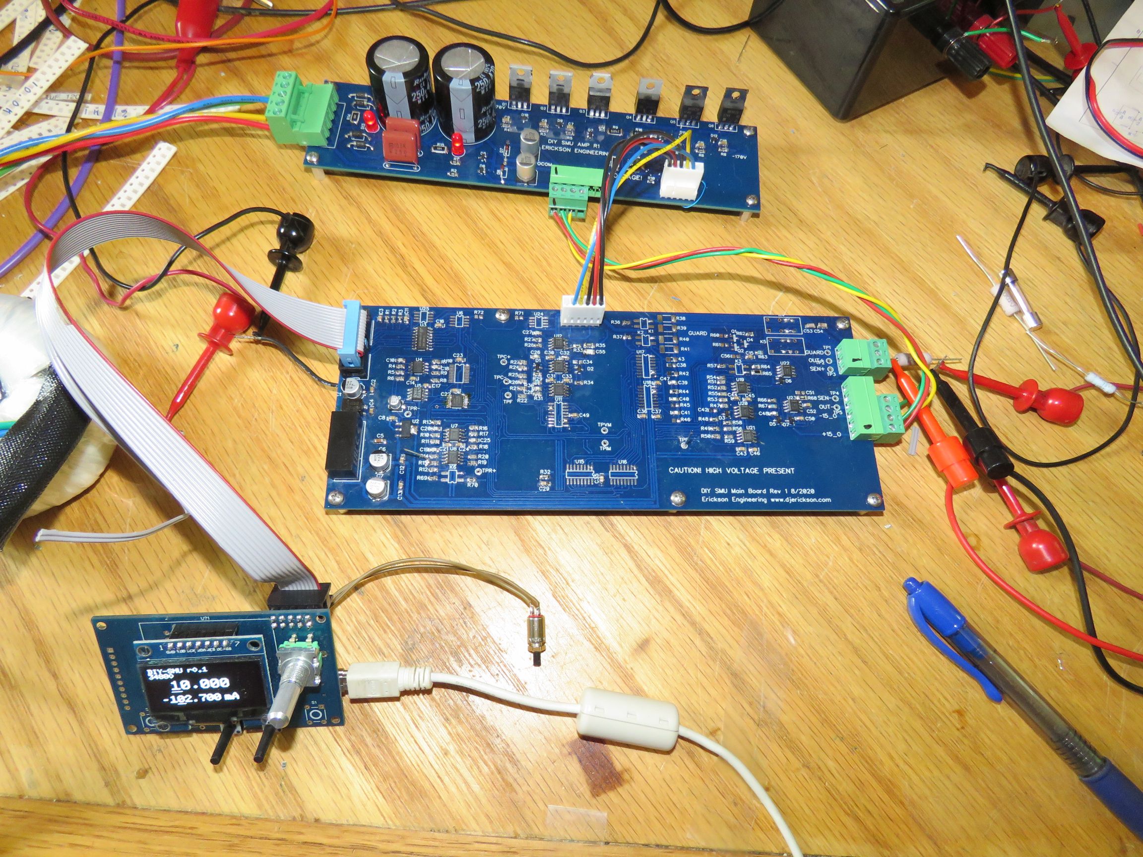
Here is the prototype as it is today. No heat sinks, and the Force
Voltage DAC is replaced by my 18b DAC box. The DAC, ADC, control
registers and current ranging switches are not installed yet. But
all the basic SMU control circuits are working.
Day 4:
This is a measurement and troubleshooting day. I
discovered that in current limit, the output oscillates with less
than ~200 ohm load. I'll try to recreate this issue in LTSpice.
The un-calibrated clamp currents are about 2-3% higher than they
should be. Since all the resistors are 0.1%, the error should be
< 1%.
The un-calibrated output voltage control is nearly perfect
however, but it increases about 0.1% when a 1mA load is applied.
Without a load, the + and - output voltages are 0.0 and -10.0
respectively, With a full scale current load applied, the outputs
are -5V and -15V. After testing a few things, I suspect that the
.1% error is due to common-mode errors of the differential
amplifier used to measure voltage. Then I remembered that there is
a common-mode calibration DAC on the '236 that I did not
implement. This is probably it. I thought that since the voltage
measurement had one output terminal close to ground, that CMRR
would not be an issue. But the +Out is not really so close to
ground. In the '236 it is up to +/- 10V. On DIY-SMU it is
+/- 5V. Without some type of common-mode correction, this will
limit the voltage set and measure accuracy of DIY-SMU. On other
designs I have implemented a trimpot for CMRR improvement. Hmmmm.
Day 5:
I improved the LTSpice simulation model to try to
simulate the oscillation with low resistance output loads. I
didn't solve the problem yet. I did a small notebook study of the
differences between DIY-SMU and the Keithley 236. I found a
compensation R-C circuit on the '236 that is not in DIY-SMU. Will
try to add it in to see if the oscillation is better.
Update: The x20 feedback network they use, 10K / 200K has a 22pF
high voltage cap across the 200K resistor. But the '236 also has a
150pF/1K (1MHz) compensation across the 200K resistor. This has
the effect of significantly reducing the high frequency gain of
the amplifier. I tried adding this circuit and presto, no
oscillation! More analysis, simulation and testing is needed.
Day 6 First firmware:
I decided to use one of my LeoLED boards to bring
up the DACs, ADCs and initial firmware. I like the way the 18b DAC
project come out, which allows a digit to be selected and then
controlled with an encoder. I re-wrote the firmware to use the new
16b DACs. The small 1.3" OLED display is a bit small to display
and control all the parameters, but I can use a small font for now
and use my reading glasses. After getting all the code to compile,
I looked at the SPI signals on the scope. It worked, but no
response from the DACs. After rechecking every pin (except Reset)
I discovered the missing pull-up resistor on RESET/. The DACs came
to life! Spent some more time getting the voltage scaling right.
Continued: firmware
Without any control bits and range switching
hardware connected, 150V is the default range. I decided when
getting the firmware going, I would use the 15V range to keep the
voltage from possibly wildly swinging around a 300V range. I
jumpered across the range set resistor, tweaked the value, and +/-
15V works fine.
It is time to clean up the old code a bunch. The 18b DAC code
worked, but it was slapped together. The display code which allows
selecting and setting the digits had many 'magic numbers'. Got to
fix that, and make the display code more general purpose. In
addition, with 9 ranges of force and 9 x 2 clamps to manage, I
need structure(s)! Also need smaller fonts to allow more stuff on
the tiny OLED. Made a simple size parameter for the display.
For each range:
- Gain and offset Cal factors for DACs and
ADCs.
- Display format for each range: Digits,
units...
- Max, Min and Init. values
- Minimum increment values
First step was to calibrate the 150V and 15V
ranges. Un-calibrated offset errors were very low, and gain errors
were under 2% as expected. With calibration the errors drop to
below 0.01%. I calibrated at +100V and 0.0V. +40.000V outputs
+39.999. +80.00 outputs +80.005. Nice!
One thing I realized: By using one DAC for both V and I Force
values, and 2 DACs for the clamps, I created more calibration
work. Because of slight differences in the DACs, resistors and
op-amps, a force voltage is slightly different from a clamp
voltage. So both need to be independently calibrated. So the
following ranges all need to be calibrated for Offset and Gain:
- 3 Voltage Force
- 6 Current +Clamp
- 6 Current - Clamp
- 6 Current Force
- 3 Voltage + Clamp
- 3 Voltage - Clamp
That's a total of 27 offset and gain
calibrations. Too much to do manually, so gotta automate this. And
most calibrations require external measurement hardware like my
trusty HP34401A 6.5 digit DMM. Python test and calibration code,
here I come.
Here is the prototype controlled by a LeoLed Arduino board. The
two buttons with tall actuators select the digit to be controlled
by the encoder. The top readout is the voltage setting. The bottom
number is just a test of a new display routine.
Next is the current ranging and ADC (measure).
ADC bringup:
Time to get the AD7190 ADC working. This is a
fairly complex SPI part requiring several 24 bit registers to be
set. These set the Clocks, Gain, Calibration, and conversion sped
which also determines the bit resolution. I am continuing to
use bit-bang SPI. When doing this I first write the code, then
scope the signals to verify the SPI SS, SCK and MOSI signals. Then
when things looked good, I installed the ADC and looked at MISO,
the data output. But I was still not getting data out of the ADC.
Delta-Sigma ADCs sample in the Hz to KHz range, so you need to
wait for the conversion to be done. This can be done by either
polling a status register or by waiting for the MISO (data output)
signal to go low.
I struggled with this for about 8 hours, then took a long look at
an Arduino Library for a very similar part, the AD7193, used on a
Diligent
PMOD ADC5 module. There is a nice Arduino library for it on
Github. The library
is a bit complex for my liking with 20 entry points. And the
library has many (12) delay() statements. In general, delay()
statements are a hack and not needed. Her library uses Hardware
SPI, but I'm currently using a lowly Leonardo with only one SPI,
which is busy doing the OLED graphics. There is probably a way to
make the SPI do other things as well, but that sounds scary to me.
So I'll stick with bit-bang SPI for now since speed isn't an
issue. By the way, when I did a hardware poly-synth with 8
channels on a Teensy, I used bit-bang SPI for 8 x 5 SPI
devices.Teensy can bit-bang SPI pretty fast if you use low-level
register controls. I do thank the author for her work on this
project without which it would have taken me a lot longer to get
this thing working. In the end I had to:
- Write a register read function to make sure
the registers were being written correctly. They weren't.
- Read and understand the example code: 10
pages, 20 entry points.
- Read and understand the AD7190 datasheet:
40 pages.
- Write a hardware reset() function that
sends 40 '1' bits. That fixed unreliable startup.
- Incorporate a proper timeout function using
a short delay(1) in a loop.
- Apply GND to unused pin 9. Not sure if this
is needed, but it's recommended.
Finally after 2 days of work, I was getting 24bit
data out! The raw ADC data is 24 bit offset-binary, and my buffer
circuit is negative polarity. I corrected for these and
applied calibration factors and finally
have an accurate +/- 150V measurement. The ADC reading noise on
the +/-150V Force/measure voltage range is about 0.5mV p-p or
0.1mV RMS. This is 300V / 0.1mV = 3e6:1
signal to noise, or 129dB SNR! Wow, very nice! This represents the low-frequency measurement
noise (~10Hz) of the the entire system:
Vref -> DAC -> Buffer ->
Crossover -> Integrator -> HiV Amp -> 2 Vsense Amps ->
HiV Diff amp -> ADC buffer -> ADC. Can't complain. High
frequency noise is also important though.
Next is to get I and V measure working and to display the measured
V and I on the OLED.
I Measure:
Adding a channel parameter to getAdc(char chan)
worked fine. I can now read out the current measurement. For added
measure I fixed the oscillation problem (see above). I added a
quickie offset and gain calibration to the only I range currently
implemented, 1mA. But when I change the voltage, I notice the
current reading increases slightly with voltage. After a few
minutes of measurements and head scratching, I realized that this
is the current drawn by my DMM due to its 10Meg input resistance.
100V / 10Meg = 10uA. This thing is actually measuring microamps on
the 1mA range very nicely, just as it should!
I Ranges:
I installed the 74HC595 shift registers that make
up the 16 bit control register. Then added an SPI function to set
these bits. These bits still don't do anything since the CMOS
switches, Photomos relays and mechanical relays are still not
installed. This made it easy to output a few test patterns without
having to worry about the effects on the hardware.
Then I removed the solder blobs that I had added to set the
current range to 1mA, and installed the Current range CMOS
switches and the other shunt resistors. I figured out all the bit
patterns to properly control the current range, voltage range, and
Mode switches. Then tested the 10uA to 10mA current ranges without
changing the display. They work well.
Top level firmware
I have all the basic hardware control functions
working. Now need to make controls for all these data structure
functions and make a UI that is user friendly Or at least not too
user-hostile. All on a tiny OLED display. Pretty big job.
struct instrument
{ // Top
level control
char mode;
//
could be enum's FV, VI, MR....
char on;
char remSense;
char iRange;
char vRange;
}
// Controls and settings for all the control values:
struct values {
float vForce;
float iClampPos;
float iClampNeg;
float iForce;
float vClampPos;
float vClampNeg;
}
// Place to keep measure values:
struct meas {
float vMeas;
float iMeas;
}
// for each range: name, units, scale factor...
struct range [NUM_RANGES] {
char[5] rangeName;
char[5] unitsName;
long scale;
}
// Calibration for each range: These need to be in EEPROM
struct cal[NUM_RANGES] {
float forceOffs;
float forceGain;
float clmpOffs;
float clmpGain;
float measOffs;
float measGain;
}
// Struct to control the display for each mode
struct disp [NUM_MODES] {
forceSet;
measDisp;
clampPSet;
clampMSet;
on_off;
remSen;
forceRange;
measRange;
settingSel;
//
select setting to control with encoder and buttons
}
I'm struggling with what processor and display to use. Leaning
towards Teensy 3.2 and Nextion LCD. I have Teensy experience
so am comfortable with using it for applications like this.
Plenty of speed and memory. But the GUI with touch screen is
scary to me. I have built a few simple monochrome LCD apps,
but nothing using a color TFT. I bought an Nextion
Display and have played with the Nextion GUI tool a bit, but
that's all. Wish me luck.
Here is a partial list of the UI functions that this project
needs:
- Large and small numerics
- Status indicators
- Scroll boxes
- Digit select and control using cursors
- Multiple screens
- Modes
- Setup
- Calibration
- Plots and graphs
- Sequencing
New GUI: Nextion
I decided Nextion was the way to go for a proper
display. They are cheap enough ($35 for a 3.5" 480x320 TFT with
touch screen) and have a nice WYSIWYG editor. I played with the
editor a bit, built up some play screens and it seemed decent. I
bought a panel and micro SD card and it seemed to work fine.
Next I installed the Nextion Arduino library, and that's where it
all went wrong. The library has dozens of examples, each with a
.HMI Nextion source
file, a .TFT Nextion executable, and a .INO Arduino source.
Perfect, right? The examples were compiled for a specific older
panel model and Arduino serial port, but those should be easy to
change, right? Then the train hit the stop: the latest Nextion
Editor, 1.61.1 won't read *any* of the example .HMI files in the
library. And the latest panels won't read *any* of the older TFT
files. Turns out all these files are 4+ years old, and they
apparently didn't think the new editor should be able to read
these older files. A bad case of version-itis and Nextion
should be ashamed. I could have tried finding an old version of
the editor, but I refuse to play that dead-end game. Turns out
that the Editor is a decent piece of software (other than not able
to read their previous version files!) but their Arduino libraries
are junk.
Fortunately the panel commands are mostly documented, and simple
enough. And a smart SW engineer, Seithan, wrote a nice simple
Nextion Library that works well. He reduced the bloated, buggy and
obsolete Nextion library to 5 simple functions. https://github.com/Seithan/EasyNextionLibrary
I was happy to donate to his PayPal. There are other web sites
that show you how to control Nextion without any libraries.
My learning curve consisted of a few days of running, learning,
and modifying Seithan's excellent examples. Soon I was able
to get a basic SMU GUI with several controls working. And get
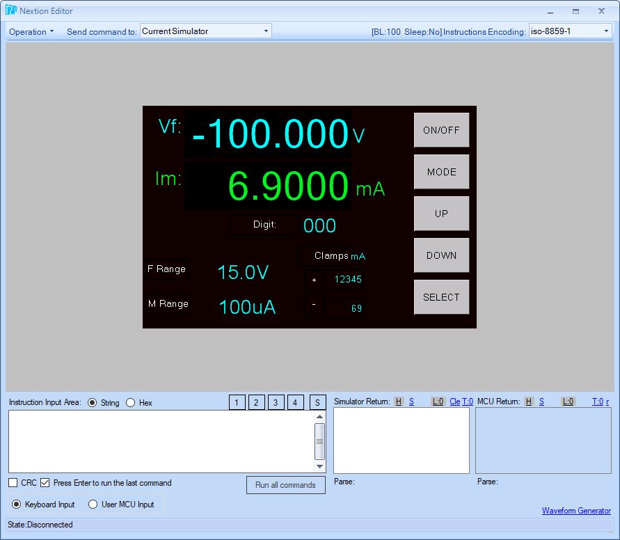
basic plotting working. Here is my prototype UI in the Nextion
simulator. Not controlling actual hardware yet, but hey, one step
at a time.
10/6/20 Update: New GUI
Thanks to some nice Nextion projects on line,
particularly uBITX, I figured out how to do a simple pull-down
menu to set the current and voltage ranges. Next is the
digit-select to show which digit is being incremented or
decremented. This took some niggling code on the OLED display to
position the underline cursor below the digits. I want it to work
for a bunch of decimal point positions on Nextion, shouldn't be
too hard to do.
It was exciting to get the hardware working with Nextion. Soon
Voltage setting and Current measure were working. Then current
range controls.
With the voltage and current ranges all working and convenient to
set, I'm getting ready to calibrate all the force ranges,
measurements, and clamps.
By the way I finally fixed the low-level oscillation issue. When I
fixed the low resistance oscillation (150KHz at 5V), a different
low-level (4MHz at 200mV)
appeared. By reducing the P gain of the PI loop, this problem went
away. I changed R27 from 10K to 2K. I was reluctant to do much
quantitative measurement while the loop was not stable. Transient
response still looks good.
Another task prior to performing calibration is to tweak the
ranges of all the DACs and ADCs. The DACs need to have enough
increased range to set the currents and voltages to the maximum
settings on each range, and to accommodate the +/- 1-2% component
tolerances. The ADC needs to do the same, including the buffer
amplifier clipping. So its buffer gain needs to be reduced a bit.
It is better to have a bit more range than to clip. Currently most
of these are set up to handle only the nominal ranges. Voltage
ranges should be +/- 150V, maybe with 2% of extra range. The
current measure is set for nominal only. Currents should be able
to set to 105% of the nominal range plus calibration, so the DACs
need about 7% of extra range.
Another consideration is auto-range. To implement auto-range, it
it is necessary that the Measurements (ADC) be able to detect when
the range is exceeded by a bit. Maybe a few extra percent of range
beyond the normal ranging. The ADC
needs this much plus a bit so I reduced the ADC input buffer gains
by about 10%. No problem since a 24 bit ADC has plenty of dynamic
range. I bought the resistors to do this but have not installed
them yet.
10/16/20 Update: 100mA, 1uA, IM Cal
Time to get all the current ranges working,
particularly 1uA and 100mA. These are the most challenging
ranges. The 1uA range is very leakage-sensitive. The total
instrument OUT+ leakage must be < 1nA as it swings +/- 5V. This
includes 7 CMOS switches, one SSR, and three op-amp bias currents.
I thought the best way to bring this up was to calibrate the 1uA
range offset and gains and see if the offset current drifted. Then
add the SSR and see if the leakage got worse. Bias and leakage
currents all get worse at high temperatures, but I'll start by
making sure they are OK at nominal room temperature. Sure enough
the currents are low and the SSR adds no measurable current, well
under 0.1nA. Good news. We'll see what happens when the
temperature rises.
I added the resistor dividers that set the short-circuit current
to the amplifier board. Without these 1K/250 ohm dividers, the
short circuit current is about 25mA. With them the current is 5 x
25mA or 125mA. I increased the current load from 10mA to 20mA,
then 50mA. The output transistors are now getting warmer. But when
I measured the 3 series power transistors, I found something
strange. At 10mA the 170V supply is pretty well balanced across
the 3 transistors: the two N-Fets and the NPN are 45V, 45V, 35V
respectively. But at 50mA they are 12V, 20V, 110V. Huh? Somewhere
above 25mA the voltages start to go haywire. I suspected
components and replaced the 2.2M resistors, then the N-FETs, but
no change.
One rule of troubleshooting: When you get crazy (unexpected)
DC values, turn on the 'scope. Sure enough there was
50-80MHz oscillation on the amplifier when the current was
increased. There is another rule that I broke with the amplifier
design: Always use series resistors on Power-FET gates. This
is because the high capacitance of the FET gates cause many
drivers to oscillate or at least ring due to trace inductance. I
first discovered this in 1978 when working with HP Labs prototype 500V powerfets.
The product failed radiated EMI due to high current ringing on the
FET gate. I added gate damping resistors and the oscillation and
EMI disappeared. I am used to oscillations causing small DC
errors, but this was causing 45V to become 12V. Why? Because a
PowerFet has a bunch of voltage gain, and 500mV of 80MHz on the
gate is enough to make them turn on pretty hard. Glad that my
scope has 100MHz bandwidth. BTW the '236 uses 50 ohm resistors on
its FET gates. Oops. The Rev2 Amp board is coming. Rev2 is my
payback for skipping a final design review on Rev1.
Then I was able to calibrate all 6 of the current measure
channels. My two bench DMMs, HP34401A and HP3478A don't have
accurate low-current ranges. They do however have good resistance
accuracy. So I selected some .01% precision resistors from my lab
stock: 1K and 10K were Vishay Metal foil. Actually these are
2K/20K networks and I use two in parallel to make 1K/10K and
increase the power handling. I have separate .1% 100K and 1M. For
10 Meg, I measured one DMM's input resistance with the other DMM
and use the 10M input resistance of the DMM as a load. Better than
nothing. I use the DMM current measure to calibrate the 100mA and
10mA ranges.
Here is my cal plan:
- Calibrate the Measure Voltage (MV) offset
and gains:
- Apply a good short circuit to the output,
run at low current (1uA) and calibrate all 3 voltage range
offsets.
- Using the DAC (uncalibrated) to output
about 1V, 10V and 100V, measure with 34401 DMM, calibrate
the VM gains.
- Calibrate the FV with either the MV or
external DMM
- With no load, calibrate Measure Current
(MI) offsets for all ranges.
- Use the FV to apply a voltage across a
precision load, calibrate MI gains
- Apply loads, calibrate Force Currents (MI)
using MV
- Apply loads, calibrate
Clamp Currents (CI) using MV
- Cal Clamp Voltages (CV) using MV
10/22/20 Update: FIMV and Clamp V Bringup
FIMV has been a long time coming. What was I
waiting for? The software to make the changes.
- User Interface to change modes and to
switch Force, Measure and Measure2
- Installed the mode CMOS switch that swaps
the force and clamp voltage measure voltages
- Wrote the control code to switch modes
- Tested V clamps with different voltages
- Tweaked FI digit and range setting.
- Added MI, FI, CI, CV to instrument data
structure
I realized (again) that my crossover absolutely
requires that the Clamp+ voltage DAC always be higher than the
Clamp-. Don't cross the streams, it
would be bad. If not, the two crossover
op-amps will fight each other, one trying to pull high and the
other low. The output will go crazy (rail to rail swings)
depending on who wins. Preventing this is one of the functions of
the constant-current diodes and bias resistors in the original
'236 crossover. Each DAC has a +/- 5.125V range or 10.5V, and I
decided to limit the difference between the two DACs to +
100mV. This is about 0.5% of the full scale range. Should be
fine.
I thought about how to control the clamps for all the different
voltage and current ranges. There will be a Clamp screen:
- Set ranges from clamp screen if needed
- Set separate V and I clamps.
- Separate FI and FV values
- If clamp > range, set for +/- range
maximum
- If clamp difference is violated, adjust the
other clamp limit to maintain minimum difference.
This way, the clamp settings will already be
established when the instrument mode is set.
11/3/20
The Clamp screen is basically working. It
requires 4 values that can be set. I decided to use one cursor
for all 4, with the < and > buttons just moving to the
next one. This isn't as simple as the Force setting since moving
past the end of one number causes the cursor to go to the next.
But the force vales don't get set so often, and it it similar
enough that a new user will figure it out quickly.
USB Control Plan: SCPI
Having a standard way to control an instrument
is important. GPIB, USB, Serial and Ethernet are all possible
hardware layers. There are many possible software layers. USB is
simple, fast, low cost and and ubiquitous. One standard
interface for test instruments is SCPI. It is an old standard,
but it is fairly simple and every test engineer is familiar with
it. Fortunately there are SCPI libraries available for Arduino.
I have not yet used them, but they look like the right tool for
this job.
Nextion Bug: Missing button events
The Nextion display was working pretty well, but
I was having trouble with missing button-press events,
particularly when changing pages.Some Nextion libraries have debug
capability. When you enable debug, a second serial port outputs
the data. I wanted to use a non-invasive way to monitor both
receive and transmit data, so bought a low cost logic analyzer,
the LA1010 for $80. It works
great and I was able to find and fix the Nextion problem in
minutes. Turns out if you tell Nextion
to update any object that is not not on the current displayed
page, it generates an error 0x1A. Generate enough of these errors
and it interferes with the Nextion trying to send event data.
Building an enclosure
As an EE, I'm perfectly happy working with
PC boards laying out on a bench or maybe attached to a piece of
sheet metal. Open breadboards make things easy to probe and
modify. But to make a useful instrument, a case is required. My
aim is to build it into a 'standard' half-rack size case: 2U
(3.5") high, 8.5" wide,and about 11-12" deep. This is the same
size as many bench-top instruments. It has front panel space for a
small touch-screen display, some controls, and the 6 Banana jacks
I need. I have searched high and low for an off-the-shelf
box this size, but found nothing. I have a few Hammond 1402F
boxes. These are close: 7.1" x 3.0" x 10.2", but are a tight
squeeze for the various parts: AC in with filter, fuse and switch,
toroid, 12V power supply, fan, heat sink, Main, Amp, and CPU
boards, front panel components, LCD and wiring. I did a
preliminary FreeCAD model and found that it could all fit if I
don't waste any space. It helps that the Hammond case has aluminum
side extrusions to help dissipate heat. I use a simple 1/4"
aluminum plate to thermally connect the transistor cases to the
box. An extra finned heat sink can be fitted if necessary.
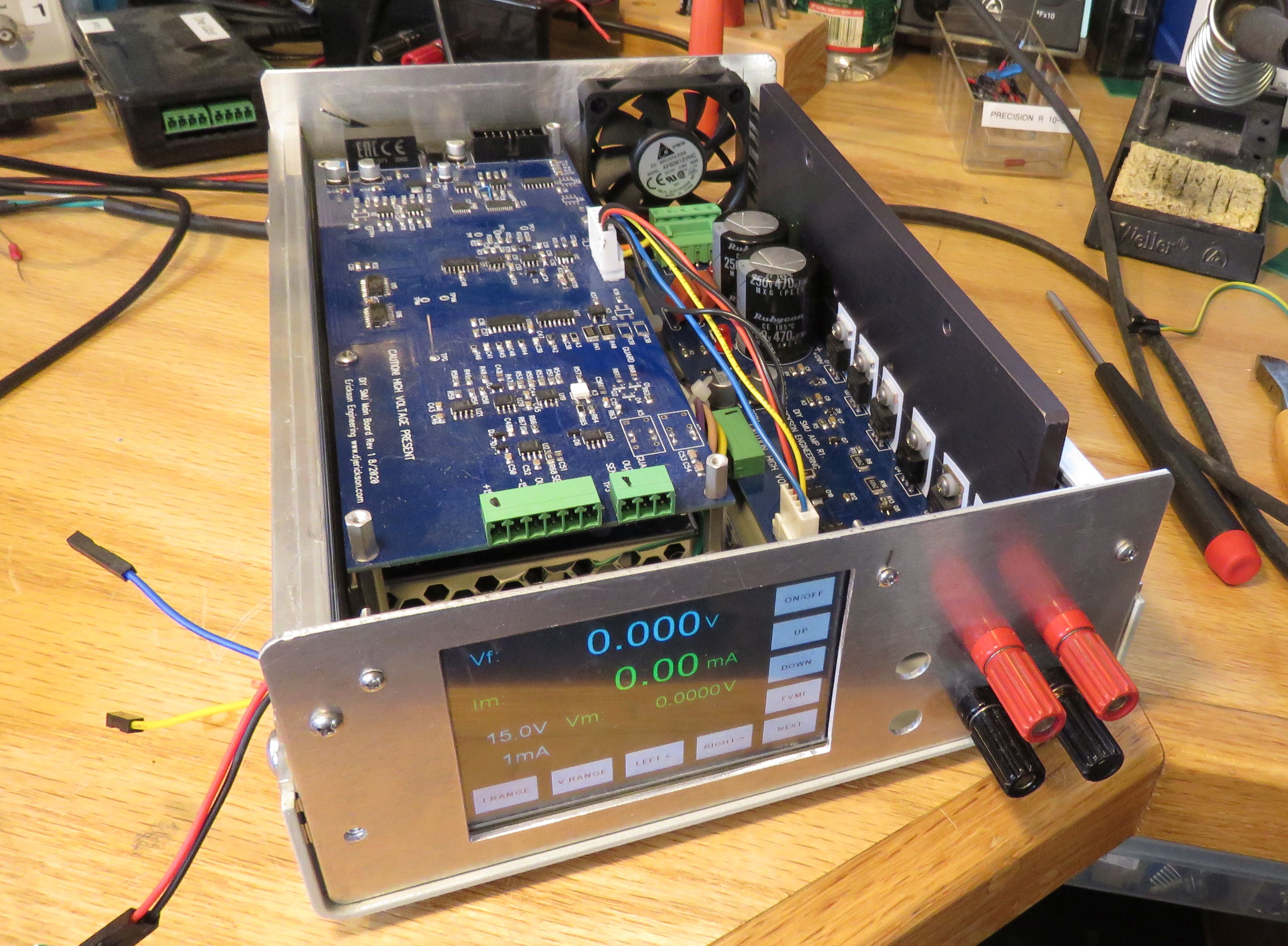
Here is DIY-SMU crammed into the Hammond box. Most parts are
installed, but not fully cabled. The Nextion LCD shows the main
startup screen but is not wired up. AC in, Toroid and 12V supply
are located below the main board. The CPU board and front
panel controls are not installed. It's getting there!
Rev2 Amp and Oscillation 11/2020
I ordered the Rev2 Amp boards and built one up.
The new board has the reworks all implemented.
- 50 ohm resistors in series with FET gates
(duh!)
- Resistor dividers on current limits to
allow 100mA
- Diodes on current limit transistor
collectors
- Fixed the lead spacing on film caps. It was
a bit short.
- Power Transistor spacing was irregular. Now
they are all 0.7" o/c to make the heat sink easier to build.
- Board length is reduced to 7.25" to better
fit small enclosures
The new amp board worked perfectly, first time.
Yay!
With all the previous oscillation issues, one still remains. The
outputs are clean if they are allowed to float. But when I ground
the -OUT, generally to the scope, the outputs oscillate at
3-400KHz and about 50mVp-p. I worked on this on-and-off for weeks,
but it remains. One problem is that the overall control loop is
complicated. It has a half a dozen opamps, plus the high voltage
amplifier. It has both voltage and current loops. I tried
improving my Spice simulation, but no. Since I needed to build up
a second unit anyway< i built one with the minimum circuitry:
no ranges or modes, voltage loop only. My plan is to reduce the
circuit complexity to the minimum that exhibits the problem.
Here's where it gets weird. Turn off the AC to the amplifier
supply: still oscillates. Disconnect the Amp board completely:
still oscillates!?! So this has nothing at all to do with he
overall loop dynamics or the amplifier. At least that narrows it
down a bunch. All that is left, and oscillation persists:
- One current range: 10mA, switching bypassed
- One voltage range, tried both 150V and 15V
- FVMI mode only: U11 is bypassed
- Changed MV amplifiers to slower and
less-precise TL07x
- No MI: Current diff amp and crossover
(Clamps) not installed. Dangerous to operate without current
limiting!No
- No Guard driver
- No ADC
- No Amplifier board so no:
- Toroid
- +/- 150V
- +/- 15V ISO: power for Out- Sense
opamp.
- Amplifier driver or output stages
- DAC is installed
- +/- 15V and +5V Power supplies and
references installed
As planned, it worked in FV mode, but the
oscillation remained. Only a handful of the opamps remain
installed: U22, U23, U19, U13, U12. These are all OPA140 or dual
OPA2140. The OPA140 series are fast 10MHz parts, and maybe
too fast. So I ordered a handful of other slower precision
JFET 5MHz amps: LF356, OP141, OP145. I can also try TL074s.
In Spice I had not simulated the gain and phase (and stability) of
each individual circuit block, so I created these models. The
Amplifier circuit works perfectly with no additional compensation.
The Voltage Measure also works, but because of filtering by the
current sense compensation caps, has a few dB peak at 300KHz. This
is a bit suspicious, close to the frequency of the oscillations.
The mystery continues....
Then I noticed that the oscillation frequency varies slightly with
the +12V input voltage. This pointed to the DC-DC power supply. I
measured the inputs to the DC-DC and saw 3V p-p of 300KHz! Finally
the problem! Turns out the Meanwell DC-DC does not like the
common-mode (CM) choke where I connected it. I removed and
bypassed it, and the output quieted considerably. Normally a
common mode choke is a good thing, reducing EMI on an output.
However in an SMU like this, that inductance plus the DC-DC
capacitance is in the ground return path. I decided the overall
design was better off without it. I replaced it with a 600ohm
ferrite in the + input only, and a short circuit in the ground.
Output turn-on relay
I installed the output relay and its driver, and
updated the firmware to control it. At least in Force Voltage
mode, it works well. However, like nearly all electro-magnetic
relays (and switches), it has contact-bounce. This appears
as an irregular turn-on waveform, lasting 10 or more milliseconds.
This can be eliminated by setting the output voltage or current to
0.0V or 0.0A prior to turning on the switch. The turn-on sequence
would be: Set Force Voltage (or current) to 0.0; turn on the
relay, wait about 50mS for the relay to turn on and stop bouncing,
then set the force V or I to the desired voltage. Or just leave
the output relay ON and set the force value to 0 instead of
turning the output OFF.
Firmware cleanup
Like most (of my) projects, the firmware has
grown organically, you know, like weeds. Currently the main force
(DAC), measure (ADC) and display functions are in-line in the main
loop() function. I have a few big features to add, and before I
add more weeds, I really should structure the main functions
better and "refactor" the code. The cleanup / refactor plan is:
- Simplify the main loop
- Make clean functions for the DAC:
setForce() and ADC: getMeasure() functions
- Create functions for setRange(),
setOutput(), setSense()...
- Clean up the display functions : Lots of
if() else()
- Clean up the command interpreter to get
ready for SCPI
- Make the ADC wait-loop non-blocking
- Prepare for the transition to Teensy
processor
- Apply the Force Cal values to the Clamps
for now. Should be ~.1% error
Then I can add the new functions:
- Plotting
- Triggering
- SCPI Interface
- Semi-automatic
Calibration
Page 1: the Analog part
Page 2: the Digital part
Page 4: Bringup Part 2
Dave's
Home Page
Last Updated:
4/24/2024